• Photonics Research
  • Vol. 5, Issue 6, 762 (2017)
Tommaso Cassese1, Marco Angelo Giambra2, Vito Sorianello2, Gabriele De Angelis2, Michele Midrio3, Marianna Pantouvaki4, Joris Van Campenhout4, Inge Asselberghs4, Cedric Huyghebaert4, Antonio D’Errico5, and Marco Romagnoli2、*
Author Affiliations
  • 1Scuola Superiore Sant’Anna-TeCIP Institute, via Moruzzi 1, 56124 Pisa, Italy
  • 2CNIT-Consorzio Nazionale Interuniversitario per le Telecomunicazioni, via Moruzzi 1, 56124 Pisa, Italy
  • 3CNIT-Consorzio Nazionale Interuniversitario per le Telecomunicazioni, Università degli Studi di Udine, 33100 Udine, Italy
  • 4Imec, Kapeldreef 75, 3001 Heverlee, Belgium
  • 5Ericsson Research, Via G. Moruzzi 1, 56124 Pisa, Italy
  • show less
    DOI: 10.1364/PRJ.5.000762 Cite this Article Set citation alerts
    Tommaso Cassese, Marco Angelo Giambra, Vito Sorianello, Gabriele De Angelis, Michele Midrio, Marianna Pantouvaki, Joris Van Campenhout, Inge Asselberghs, Cedric Huyghebaert, Antonio D’Errico, Marco Romagnoli. Capacitive actuation and switching of add–drop graphene-silicon micro-ring filters[J]. Photonics Research, 2017, 5(6): 762 Copy Citation Text show less
    (a) Schematic of the SOG capacitor waveguide. (b) Top view (not to scale) of the proposed device. Gray shapes are silicon waveguides, dark gray is the highly p-doped silicon slab, green is graphene, and yellow marks the contacts.
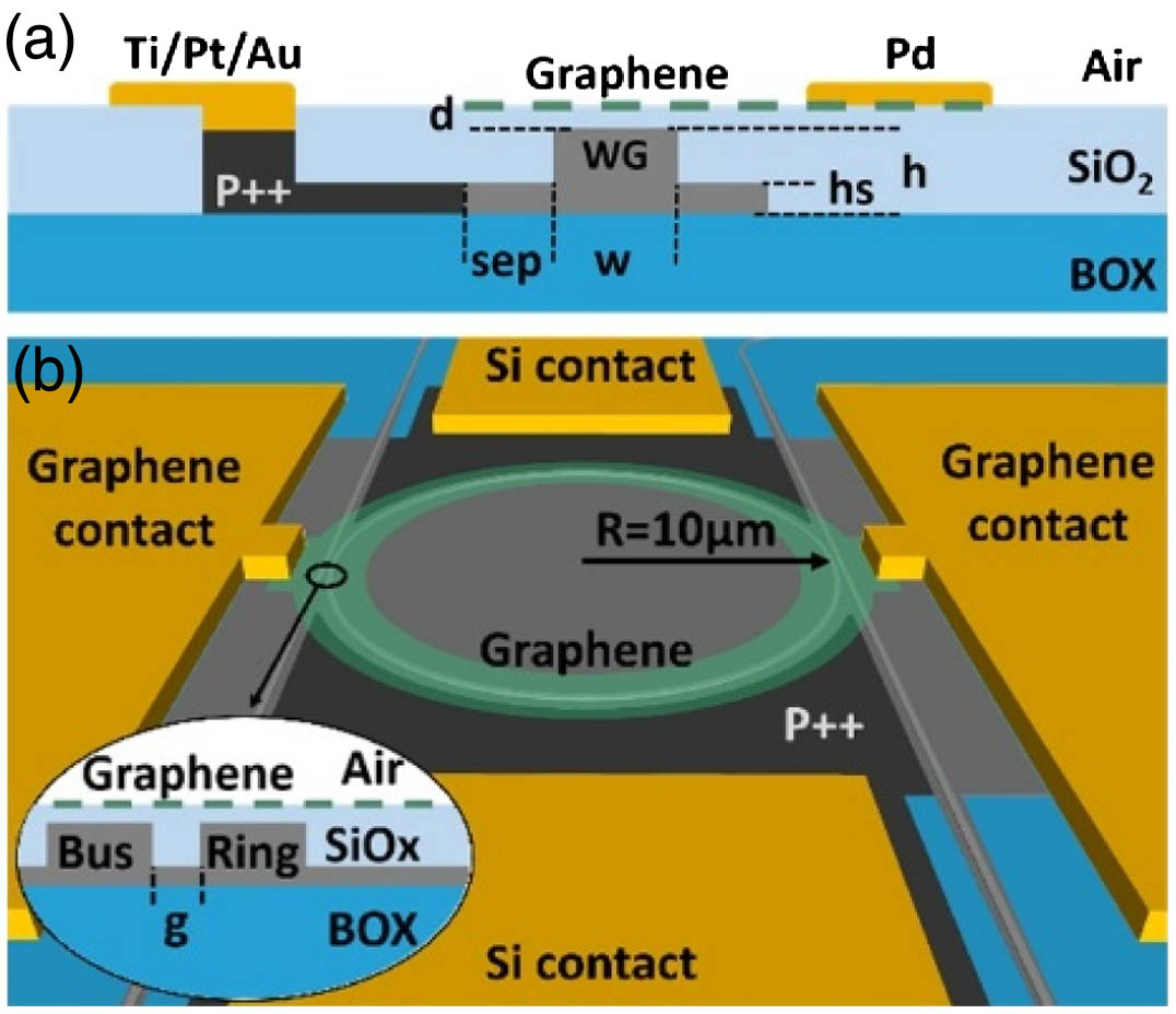
    Fig. 1. (a) Schematic of the SOG capacitor waveguide. (b) Top view (not to scale) of the proposed device. Gray shapes are silicon waveguides, dark gray is the highly p-doped silicon slab, green is graphene, and yellow marks the contacts.
    Optical micrograph picture of the device. Inset shows a detail of the MRR.
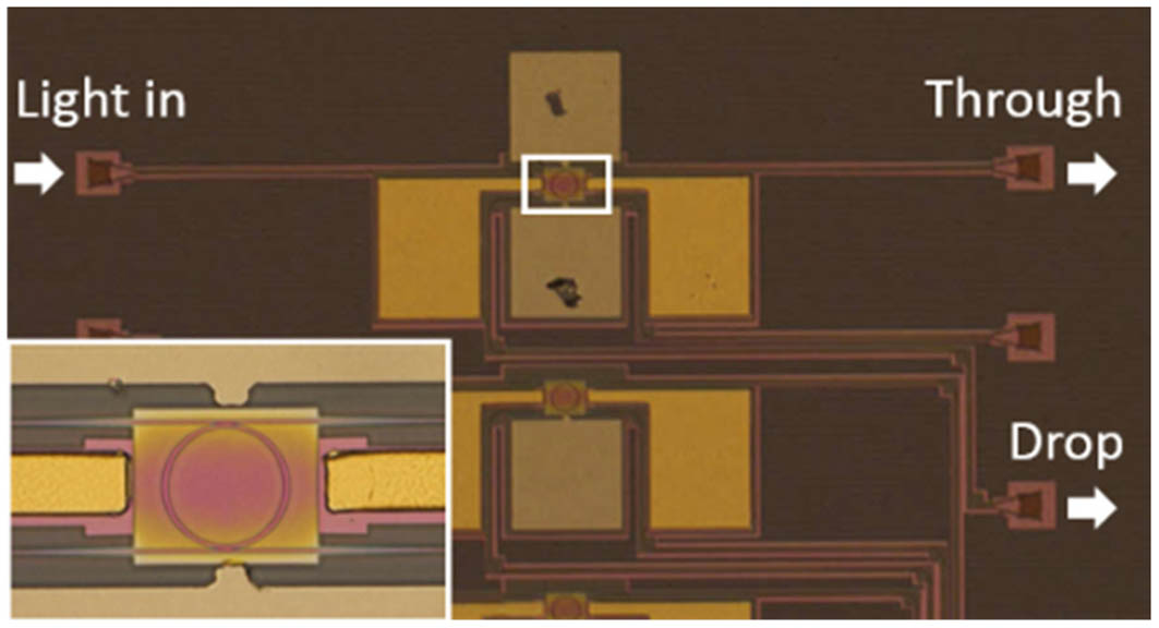
    Fig. 2. Optical micrograph picture of the device. Inset shows a detail of the MRR.
    Absorption and effective index of the SOG loaded waveguide at 1.55 μm versus the graphene Fermi level. Blue and red curves are for τ=300 and 30 fs, respectively.
    Fig. 3. Absorption and effective index of the SOG loaded waveguide at 1.55 μm versus the graphene Fermi level. Blue and red curves are for τ=300 and 30  fs, respectively.
    Simulated transmission at the through (solid lines) and drop (dashed lines) ports of the MRR for different graphene scattering times: (a) τ=30 and (b) 300 fs. Different colors refer to different values of the Fermi level of graphene: black is for μ=0.3 eV, red for μ=0.4 eV, and blue for μ=0.5 eV.
    Fig. 4. Simulated transmission at the through (solid lines) and drop (dashed lines) ports of the MRR for different graphene scattering times: (a) τ=30 and (b) 300  fs. Different colors refer to different values of the Fermi level of graphene: black is for μ=0.3  eV, red for μ=0.4  eV, and blue for μ=0.5  eV.
    Computed graphene Fermi level as a function of the V–VDirac voltage.
    Fig. 5. Computed graphene Fermi level as a function of the VVDirac voltage.
    Experimental through (solid lines) and drop (dashed lines) transmission spectra for different VGS values. Black curves for VGS=14 V (switch disabled), red curves for VGS=0 V (switch is enabling), and blue curves for VGS=14 V (switch enabled).
    Fig. 6. Experimental through (solid lines) and drop (dashed lines) transmission spectra for different VGS values. Black curves for VGS=14  V (switch disabled), red curves for VGS=0  V (switch is enabling), and blue curves for VGS=14  V (switch enabled).
    Tommaso Cassese, Marco Angelo Giambra, Vito Sorianello, Gabriele De Angelis, Michele Midrio, Marianna Pantouvaki, Joris Van Campenhout, Inge Asselberghs, Cedric Huyghebaert, Antonio D’Errico, Marco Romagnoli. Capacitive actuation and switching of add–drop graphene-silicon micro-ring filters[J]. Photonics Research, 2017, 5(6): 762
    Download Citation