Abstract
We propose and experimentally demonstrate capacitive actuation of a graphene–silicon micro-ring add/drop filter. The mechanism is based on a silicon–SiO2–graphene capacitor on top of the ring waveguide. We show the capacitive actuation of the add/drop functionality by a voltage-driven change of the graphene optical absorption. The proposed capacitive solution overcomes the need for continuous heating to keep tuned the filter’s in/out resonance and therefore eliminates “in operation” energy consumption.1. INTRODUCTION
Photonic switching is one of the fundamental topics of integrated optics. Thanks to development in the field of silicon photonics, reaching high miniaturization and low cost, silicon and silicon nitride () optical add and drop multiplexers (OADMs) based on micro-ring resonators (MRRs) currently offer perspectives [1,2], in particular for access networks that require large volumes [3]. The add/drop functionality of a silicon photonic OADM can be switched by properly tuning or detuning the MRR resonance with respect to the signal wavelength. In particular, switching is achieved by exploiting the thermo-optic effect by means of metallic or Si-based Joule heaters integrated in close proximity of the MRR waveguide. Although the thermo-optic effect is very efficient in silicon, the thermo-optic actuation requires continuous power consumption that can easily sum to some milliwatts [4]. In a complex switching matrix with tens or more MRRs, this power consumption can be detrimental. Moreover, this approach may limit the wavelength channel density in wavelength-division-multiplexing (WDM) systems. In fact, the thermo-optic actuation implies that the MRR resonance must be tuned to a wavelength in the center between two adjacent channels in order to avoid crosstalk. Depending on the shape of the MRR resonance, the detuned wavelength may set a limit to the minimum grid separation. Switching could also be achieved by using free-carrier effect modulators, either in depletion p–n junctions or in injection p-i-n junctions, or in a semiconductor–insulator–semiconductor capacitor (SISCAP) configuration [5]. However, depletion p–n junctions and SISCAP modulators allow for only resonance detuning, thus limiting the channel density, whereas large variation of optical losses can be obtained with carrier injection in p-i-n junctions, but at the cost of large power consumption (of the order of hundreds of milliwatts) due to forward bias current [6]. For these reasons, alternative approaches are needed for add/drop switching, e.g., suppressing the resonance rather than relying on thermal tuning/detuning.
Graphene is a versatile 2D material with tunable optical properties allowing large spectral bandwidth, high speed, small footprint, and CMOS compatibility. Graphene has recently raised interest for application in photonics integrated circuits [7]. Graphene–on–Si modulators and photodiodes have already been successfully demonstrated [8–11]. These devices exploit the possibility of large tuning of the complex optical conductivity of graphene by electrical gating [12]. The in-plane complex optical conductivity of graphene can be expressed as a function of the Fermi level as [13] Here, is the universal conductivity of graphene (with the electron charge), is the Fermi level energy, the thermal energy, the photon energy, and the intra-band scattering time [14]. Given a capacitor structure where graphene is one of the plates, the Fermi level may be varied by carrier accumulation on the graphene layer by applying an external voltage [15]. The applied voltage will result as the sum of two terms: the first is the potential across the capacitor dielectric, the second is due to the Fermi potential shift induced by the accumulated carriers on the graphene layer. This relation is expressed as [16] Here, is the oxide capacitance per unit area, is the graphene surface carrier density, is the Fermi velocity [14], and is the flat-band voltage of the charge-neutral Dirac point. The flat-band voltage is a fabrication-dependent parameter affected by the built-in doping of the graphene monolayer.
In this paper, we propose a silicon reconfigurable add/drop filter with an integrated switching element based on an –graphene (silicon-oxide-graphene, SOG) capacitor. The novelty and advantage of the proposed device with respect to state-of-the-art MRRs consists of the physical mechanism at the basis of the switching operation. In particular, we disable and enable the resonance by absorbing the light in the MRR by electro-absorption through graphene. This allows avoiding the crosstalk issues introduced by the simple thermal tuning/detuning of the MRR resonance. Moreover, the graphene absorption is changed by tuning the Fermi level through the SOG capacitor, i.e., by means of a capacitive mechanism. This leads to negligible power consumption with respect to the more power hungry Joule effect of thermo-optic-based switching. Moreover, the power consumption of the proposed switches occurs only during the charge and discharge of the SOG capacitor, whereas in the case of thermo-optic effect the current flow is continuous.
Sign up for Photonics Research TOC. Get the latest issue of Photonics Research delivered right to you!Sign up now
2. FABRICATION
The proposed MRR filter is based on a silicon-on-insulator (SOI) ridge waveguide with core width , core height , and slab height . The Si waveguide is top cladded with . The planarized top cladding is 230 nm thick, i.e., on top of the waveguide core. Graphene is transferred on the surface on both the ring and bus waveguides. The cladding on top of the graphene layer is air. The SOG capacitor stack is constituted by the silicon waveguide, the 10 nm layer, and graphene. The computed capacitance per unit area is . Figure 1(a) shows a schematic cross section of the proposed waveguide with the SOG capacitor.
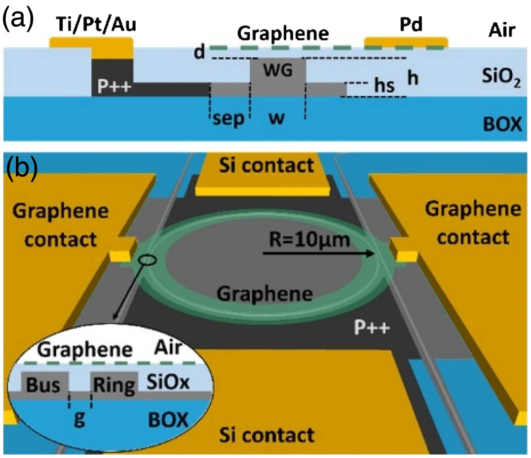
Figure 1.(a) Schematic of the SOG capacitor waveguide. (b) Top view (not to scale) of the proposed device. Gray shapes are silicon waveguides, dark gray is the highly p-doped silicon slab, green is graphene, and yellow marks the contacts.
The waveguide cores and part of the slab layer (gray) is lightly p-doped (), whereas the remaining part of the slab (dark gray) is highly p-doped () to obtain ohmic contacts. The distance between the high-doped region and the waveguide core was set to to avoid extra optical losses in the MRR. Graphene is patterned to cover the MRR and part of the buses (green in Fig. 1). The proposed MRR has radius and coupling regions with gap between the access bus and ring waveguides. Figure 1(b) shows a schematic top view of the designed MRR.
The silicon photonic chip was fabricated on the IMEC iSiPP25G SOI platform [17]. Graphene was grown by means of chemical vapor deposition on copper foils [18], and then transferred onto the chip by the process described in Ref. [19]. The graphene patterning was done by using a stack of polymethyl methacrylate (PMMA) and IX845 protecting it during plasma etching. The graphene contacts consist of 50 nm of palladium (Pd), while the contact on Si is a stack of titanium/platinum/gold (Ti/Pt/Au 20/20/30 nm).
Figure 2 shows an optical microscope picture of the fabricated device. In the picture can be noted the MRR covered by graphene (not visible), the contact pads, and four input/output single polarization grating couplers (GCs) used to inject/extract light from the four ports of the filter. The inset shows a detail of the MRR.

Figure 2.Optical micrograph picture of the device. Inset shows a detail of the MRR.
3. NUMERICAL ANALYSIS
For a more comprehensive analysis of the device, we simulated its behavior considering two values of graphene scattering time: and (corresponding to mobility and , respectively, at ) illustrating the effect of this parameter on the waveguide absorption and dispersion. As we show below, is the best fitting parameter for the experimental data. A commercial-grade simulator eigenmode solver and propagator was used to perform the calculations of the effective index, group index, and optical absorption of the graphene-on-Si waveguide [20]. Relative dielectric constants at optical frequencies of Si and were set to and , respectively. Graphene was treated as an equivalent 3D material of thickness [21], having the out-of-plane dielectric constant of graphite equal to 5.7, and in-plane dielectric constant given by with given by Eq. (1). In the simulations, we included the effect of free carriers in Si according to Soref’s formulas [22]. Figure 3 shows the effective index and absorption of the designed SOG loaded waveguide [cross section shown in Fig. 1(a)] as a function of the graphene Fermi level at the free space wavelength .
Figure 3.Absorption and effective index of the SOG loaded waveguide at 1.55 μm versus the graphene Fermi level. Blue and red curves are for and , respectively.
When the Fermi level of graphene is below half the photon energy (, where at 1.55 μm), the waveguide absorption is greater than . Conversely, when , optical absorption drops down and bounds to a minimum level that is strongly affected by the intra-band scattering mechanisms [16] ( to for and ). The effective index slowly decreases when , then increases with a peak at , and then monotonically decreases for increasing Fermi level in the low-loss region for .
We also evaluated the coupling coefficient between the bus and MRR waveguides for gap , ring radius , and , which is . The results extracted from the mode analysis were used to simulate the fabricated MRR. A commercial-grade circuit simulator for the design, simulation, and analysis of photonic integrated circuits was used to perform the calculations [20]. To compare the numerical results with the experimental measurements, we included in the simulations the insertion losses of the input and output GCs, which was experimentally estimated at 10 dB. Figure 4 shows the numerically computed spectra at the through and drop ports of the MRR [see Fig. 2(b) for the port positions]. Figures 4(a) and 4(b) are for and , respectively. The solid lines are the transmission spectra at the through port, while the dashed lines are transmission values at the drop port. Black, red, and blue are used for Fermi levels , 0.4, and 0.5 eV, respectively.
Figure 4.Simulated transmission at the through (solid lines) and drop (dashed lines) ports of the MRR for different graphene scattering times: (a) and (b) . Different colors refer to different values of the Fermi level of graphene: black is for , red for , and blue for .
The resonance of the MRR is enabled when graphene is in the low-loss condition (), while it is disabled when the Fermi level is tuned in the high-loss condition (). In particular, if the single round-trip loss is large enough, waves cannot add coherently inside the ring and the resonance is suppressed. This is the case of the black curves in Fig. 4, which refer to the Fermi level . In this condition, the incoming light is directed toward the through port, with an insertion loss that depends on the length of the MRR cavity and the absorption induced by the SOG. For the designed device (10 μm radius), the expected insertion loss is (see Fig. 4, solid black curve). For longer devices, i.e., when the light inside the cavity is completely absorbed at the first round trip, the insertion loss corresponds to the light lost in the coupling region, in the designed coupling region (11% coupling). When graphene is driven to its low-loss condition (blue curve in Fig. 4, ), waves can develop interference arising from multiple round trips inside the MRR cavity, eventually directing resonant frequencies to the drop port. In this condition, the insertion loss at the drop port depends on the background propagation loss inside the MRR cavity. This is highly dependent on the scattering time , i.e., the quality of graphene, as shown in Fig. 3. In particular, the waveguide absorption at 0.5 eV changes from to for and , respectively. With these values, the drop loss for is at the resonant wavelengths, with an extinction at the through port of . This performance can be significantly improved by using a graphene with higher mobility, i.e., longer scattering time. In fact, we evaluated a drop loss of at the resonant wavelengths for , with an extinction at the through port of .
The graphene Fermi level is tuned by means of the SOG capacitor according to Eq. (2). Applying a voltage to the SOG, charges are accumulated on the SOG plates, causing the tuning of the graphene Fermi level. Figure 5 shows the Fermi level as a function of the voltage applied on the graphene plate, as computed with Eq. (2). Since the silicon waveguide is p-doped, the is negative to induce accumulation of electrons on graphene and holes on Si. To set the Fermi level , we need a bias voltage between the graphene (G) and Si (S) contacts, . Taking into account the capacitance per unit area of the SOG capacitor (), the area of the capacitor A , and the voltage needed to bring the graphene to transparency condition, we computed the switching energy to enable the filter to be .
Figure 5.Computed graphene Fermi level as a function of the voltage.
4. EXPERIMENTAL RESULTS
For the experimental characterizations, we used a tunable external cavity laser (ECL) emitting in the C-band, a power monitor to collect the output power from the drop port and the through port, and four electrical probes to contact the electrical pads. Figure 6 shows the experimental transmission spectra at the through (solid lines) and drop (dashed lines) ports for different values of the applied .
Figure 6.Experimental through (solid lines) and drop (dashed lines) transmission spectra for different values. Black curves for (switch disabled), red curves for (switch is enabling), and blue curves for (switch enabled).
In all the measurements, the input power is 0 dBm. The overall insertion loss due to the input and output GCs is 10 dB (5 dB each). Applying to the SOG, the drop port is disabled and we measured the maximum extinction ratio (ER) between the through and drop ports at the MRR resonance wavelength, i.e., . On the through port, a residual effect of the MRR is barely visible and accounts for a through loss of 1.5 dB. According to simulations, this operating point corresponds to Fermi level close to 0 eV, which means that the experimental . Conversely, to enable the drop port, we decreased down to (blue curves), obtaining maximum output power at resonance of , with an ultimate drop loss of with respect to the through port transmission off resonance. Further lowering the caused dielectric breakdown of the layer. The experimental range was 28 V, i.e., larger than expected. In particular, the switching from the absorbing to the transparent condition of graphene, e.g., the range from 0 to 0.5 eV, was expected to be achieved within swing (see Fig. 5). We ascribe this to the small leakage current () flowing through the dielectric between the graphene and the Si. This small current causes a voltage drop on the ungated graphene and on the low doped silicon, reducing the effective voltage on the SOG capacitor plates. The experimental measurements fitted very well with the numerical simulations of Fig. 4(a), allowing an estimation of the scattering time of 30 fs. This is the main limiting factor to the switching performance of the fabricated device; better quality graphene would have fitted the curves in Fig. 4(b).
5. CONCLUSIONS
We proposed a novel mechanism for optical switching add/drop filters based on MRRs. The physical mechanism responsible for switching is electro-absorption rather than electro-refraction as in conventional add/drop MRRs. The effect is enabled by graphene on a silicon photonic waveguide. When graphene is driven to high or low loss, the resonance of the MRR is suppressed or enabled, respectively, allowing switching of the add–drop functionality. The proposed switching scheme avoids the adjacent channel crosstalk issues typically introduced by the simple thermal tuning/detuning of the MRR resonance. Moreover, since graphene is gated by means of a capacitive element (SOG capacitor), the proposed scheme is able to perform switching with power consumption only during switching time and no consumption during static operation. This is to be compared to the conventional detuning obtained by the power hungry Joule effect.
References
[1] T. Barwicz, M. R. Watts, M. A. Popović, P. T. Rakich, L. Socci, F. X. Kärtner, E. P. Ippen, H. I. Smith. Polarization-transparent microphotonic devices in the strong confinement limit. Nat. Photonics, 1, 57-60(2007).
[2] M. S. Dahlem, C. W. Holzwarth, A. Khilo, F. X. Kärtner, H. I. Smith, E. P. Ippen. Reconfigurable multi-channel second-order silicon microring-resonator filterbanks for on-chip WDM systems. Opt. Express, 19, 306-316(2011).
[3] V. Sorianello, G. De Angelis, T. Cassese, M. V. Preite, P. Velha, A. Bianchi, M. Ronmagnoli, F. Testa. Polarization insensitive silicon photonics ROADM with selectable communication direction for radio access network. Opt. Lett., 41, 5688-5691(2016).
[4] K. Padmaraju, K. Bergman. Resolving the thermal challenges for silicon microring resonator devices. Nanophotonics, 3, 269-281(2013).
[5] G. T. Reed. Silicon Photonics: The State of the Art(2008).
[6] S. Park, K. Yamada, T. Tsuchizawa, T. Watanabe, H. Shinojima, H. Nishi, R. Kou, S. Itabashi. Influence of carrier lifetime on performance of silicon p-i-n variable optical attenuators fabricated on submicrometer rib waveguides. Opt. Express, 18, 11282(2010).
[7] F. Bonaccorso, Z. Sun, T. Hasan, A. C. Ferrari. Graphene photonics and optoelectronics. Nat. Photonics, 4, 611-622(2010).
[8] M. Liu, X. Yin, E. Ulin-Avila, B. Geng, T. Zentgraf, L. Ju, F. Wang, X. Zhang. A graphene-based broadband optical modulator. Nature, 474, 64-67(2011).
[9] F. H. Koppens, T. Muller, P. Avouris, A. C. Ferrari, M. S. Vitiello, M. Polini. Photodetectors based on graphene, other two-dimensional materials and hybrid systems. Nat. Nanotechnol., 9, 780-793(2014).
[10] Y. T. Yu, M. Pantouvaky, S. Brems, I. Asselberghs, C. Huyghebaert, M. Geisler, C. Alessandri, R. Baets, P. Absil, D. Van Thourhout, J. Van Campenhout. Broadband 10 Gb/s graphene electro-absorption modulator on silicon for chip-level optical interconnects. IEEE International Electron Devices Meeting (IEDM), 128-131(2014).
[11] V. Sorianello, M. Midrio, G. Contestabile, I. Asselberg, J. Van Campenhout, C. Huyghebaerts, I. Goykhman, A. K. Ott, A. C. Ferrari, M. Romagnoli. Graphene phase modulators(2017).
[12] V. Sorianello, G. De Angelis, T. Cassese, M. Midrio, M. Romagnoli, M. Moshin, M. Otto, D. Neumaier, I. Asselberghs, J. Van Campenhout, C. Huyghebaert. Complex effective index in graphene-silicon waveguides. Opt. Express, 24, 29984(2016).
[13] Y.-C. Chang, C.-H. Liu, C.-H. Liu, Z. Zhong, T. B. Norris. Extracting the complex optical conductivity of mono- and bilayer graphene by ellipsometry. Appl. Phys. Lett., 104, 261909(2014).
[14] S. Das Sarma, S. Adam, E. H. Hwang, E. Rossi. Electronic transport in two-dimensional graphene. Rev. Mod. Phys., 83, 407-470(2011).
[15] J. Yan, Y. Zhang, P. Kim, A. Pinczuk. Electric field effect tuning of electron-phonon coupling in graphene. Phys. Rev. Lett., 98, 166802(2007).
[16] V. Sorianello, M. Midrio, M. Romagnoli. Design optimization of single and double layer graphene phase modulators in SOI. Opt. Express, 23, 6478-6490(2015).
[17] P. P. Absil, P. De Heyn, H. Chen, P. Verheyen, G. Lepage, M. Pantouvaki, J. De Coster, A. Khanna, Y. Drissi, D. Van Thourhout, J. Van Campenhout. Imec iSiPP25G silicon photonics: a robust CMOS-based photonics technology platform. Proc. SPIE, 9367, 93670V(2015).
[18] X. Li, W. Cai, J. An, S. Kim, J. Nah, D. Yang, R. Piner, A. Velamakanni, I. Jung, E. Tutuc, S. K. Banerjee, L. Colombo, R. S. Ruoff. Large-area synthesis of high-quality and uniform graphene films on copper foils. Science, 324, 1312-1314(2009).
[19] A. Zurutuza, A. Centeno, B. Alonso, A. Pesquera. Method of manufacturing a graphene monolayer on insulating substrates. U.S. patent(2015).
[20] Lumerical Solutions,.
[21] Y. Huang, J. Wu, K. C. Hwang. Thickness of graphene and single-wall carbon nanotubes. Phys. Rev. B, 74, 245413(2006).
[22] M. Nedeljkovic, R. Soref, G. Z. Mashanovich. Free-carrier electrorefraction and electroabsorption modulation predictions for silicon over 1-14 micron infrared wavelength range. IEEE Photon. J., 3, 1171-1180(2011).


