
Yixuan Zhu, Shenqiang Zhai, Kun Li, Kai Guo, Qiangqiang Guo, Jinchuan Zhang, Shuman Liu, Lijun Wang, Fengqi Liu, Junqi Liu. Mode-switchable dual-color infrared quantum cascade detector[J]. Photonics Research, 2024, 12(2): 253
- Photonics Research
- Vol. 12, Issue 2, 253 (2024)
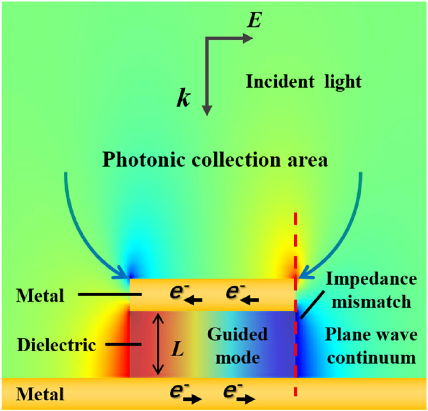
Fig. 1. Illustration of a patch antenna. The figure shows the simulated vertical component of the distribution of the electric field E z
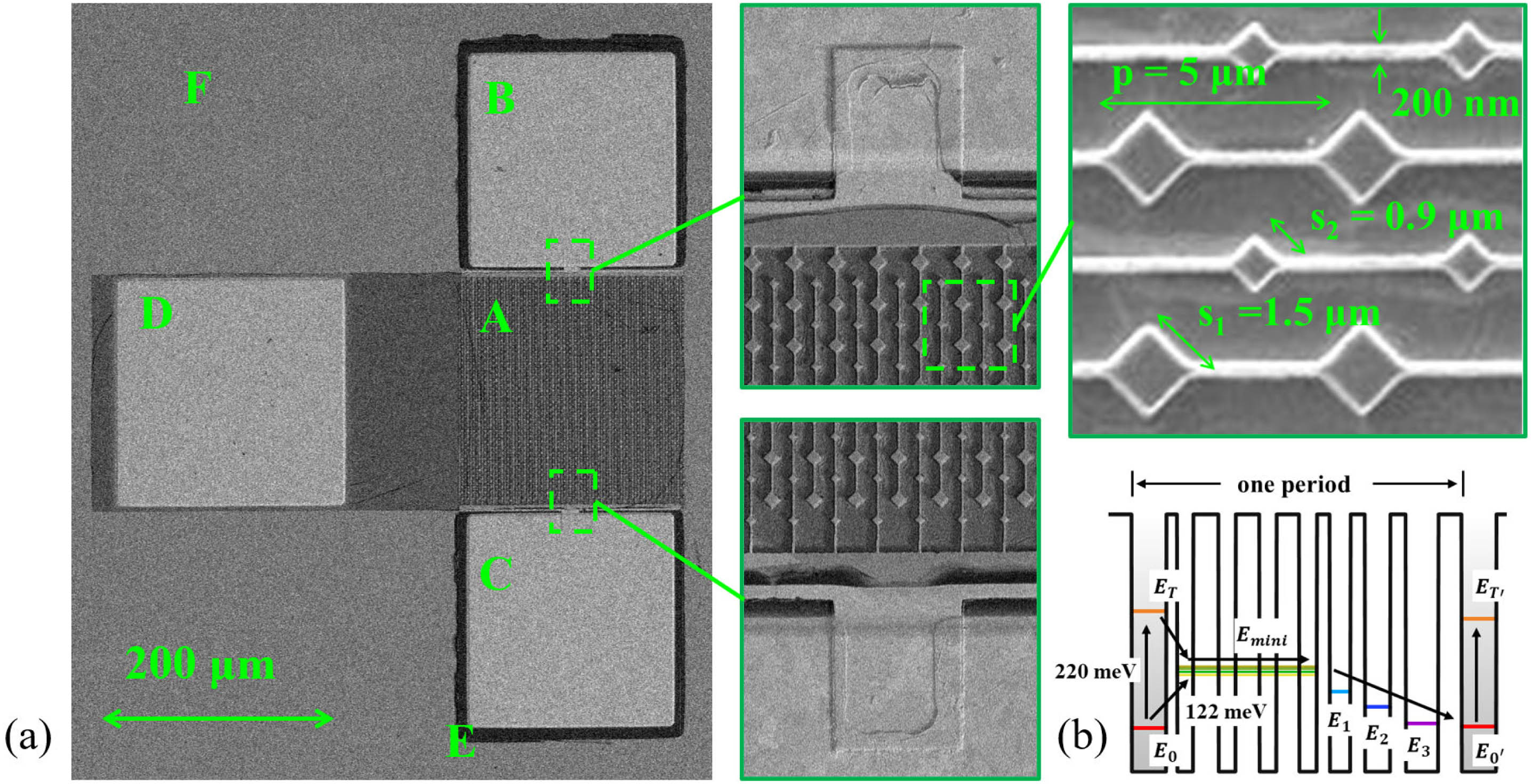
Fig. 2. (a) Scanning electron microscope image of the detector, with partial enlargements of the electrically connected patch antennas. The main parameters of the array are indicated in the diagram. Region A: the photonic collection area. Region B: the top metal electrode for the 10.0-μm channel. Region C: the top metal electrode for the 5.7-μm channel. Region D: the bottom metal electrode. Region E: SiO 2
Fig. 3. (a) Respectively normalized simulated distribution of the absolute vertical component of the electric field | E z |
Fig. 4. (a) Normalized responsivity spectrum of the device at 77 K and zero bias, in the case of unpolarized incident light. (b) Peak responsivity of the device as a function of temperature. (c) Detectivity of the device as a function of temperature. From left to right, the device works in dual-color, long-wave, and mid-wave modes sequentially.
Fig. 5. (a) Normalized responsivity spectrum of the detector as a function of the polarization angle of the incident light, at 77 K and zero bias. (b) Peak responsivity as a function of the polarization angle, at 77 K and zero bias. From left to right, the device works in dual-color, long-wave, and mid-wave modes, respectively.
Fig. 6. Ratio of the peak responsivity of the two channels as a function of the polarization angle.
Fig. 7. Partial enlargement of the electrically connected patch antennas of the “Patch-Parallel” device.
Fig. 8. Peak responsivity of the “Patch-Parallel” device as a function of the polarization angle, at 77 K and zero bias. From left to right, the device works in dual-color, long-wave, and mid-wave modes, respectively.
Fig. 9. Ratio of the peak responsivity of the “Patch-Parallel” device of the two channels as a function of the polarization angle.

Set citation alerts for the article
Please enter your email address
© Copyright 2018-2021 | Chinese Laser Press. All Rights Reserved 沪ICP备15018463号-20