• Photonics Research
  • Vol. 12, Issue 2, 253 (2024)
Yixuan Zhu1、2, Shenqiang Zhai1、2、3, Kun Li1、2, Kai Guo1、2, Qiangqiang Guo1、2, Jinchuan Zhang1、2, Shuman Liu1、2, Lijun Wang1、2, Fengqi Liu1、2, and Junqi Liu1、2、*
Author Affiliations
  • 1Key Laboratory of Semiconductor Materials Science, Beijing Key Laboratory of Low Dimensional Semiconductor Materials and Devices, Institute of Semiconductors, Chinese Academy of Sciences, Beijing 100083, China
  • 2Center of Materials Science and Optoelectronics Engineering, University of Chinese Academy of Sciences, Beijing 100049, China
  • 3e-mail: zsqlzsmbj@semi.ac.cn
  • show less
    DOI: 10.1364/PRJ.509686 Cite this Article Set citation alerts
    Yixuan Zhu, Shenqiang Zhai, Kun Li, Kai Guo, Qiangqiang Guo, Jinchuan Zhang, Shuman Liu, Lijun Wang, Fengqi Liu, Junqi Liu. Mode-switchable dual-color infrared quantum cascade detector[J]. Photonics Research, 2024, 12(2): 253 Copy Citation Text show less

    Abstract

    In this paper, a patch-antenna-array enhanced quantum cascade detector with freely switchable operating modes among mid-wave, long-wave, and dual-color was proposed and discussed. The dual-color absorption occurs in a single active region through an optimized coupled miniband diagonal-transition subbands arrangement, and a successful separation of the operation regimes was realized by two nested antenna arrays with different patch sizes up to room temperature. At 77 K, the 5.7-μm channel achieved a peak responsivity of 34.6 mA/W and exhibited a detectivity of 2.0×10¹⁰ Jones, while the 10.0-μm channel achieved a peak responsivity of 87.5 mA/W, giving a detectivity of 5.0×10¹⁰ Jones. Under a polarization modulation of the incident light, the minimum cross talk of the mid-wave and the long-wave operating modes was 1:22.5 and 1:7.6, respectively. This demonstration opens a new prospect for multicolor infrared imaging chip integration technology.

    1. INTRODUCTION

    Over the past few decades, extraordinary progress has been made in the field of infrared imaging technology, much of which can be attributed to dramatic advances in the analysis and processing of infrared sensor manufacturing [1]. The next generation of infrared imaging systems requires a larger number of pixels, faster frame rates, higher sensitivity, elevated operating temperatures, and multicolor functionality [24]. Among the many requirements, the capability of dual-color/multicolor detection is particularly important. Multispectral detection or simultaneous collection of signals from different infrared bands provides enhanced target discrimination and identification, and has attracted increased interest [5,6]. In this region, the quantum cascade detector (QCD) is a very competitive candidate, but barely exploited. Confined by the ladder-shaped subbands arrangement, the photoexcited transitions in QCDs are complicated. It allows the absorption of several colors to occur in a single active region [710]. As a consequence of the bound-to-bound optical transition, each photoresponse peak is sharp, clear, and has no overlap with others. Conventional multicolor detectors have to work with external bias [11,12], and therefore, the signals from different channels have to be output in sequence. However, thanks to the asymmetric intersubband (ISB) structure, QCDs are photovoltaic devices [1315], and the signals of several channels can be output independently as well as simultaneously. In addition, operating with zero bias avoids mutual electrical interference among different channels, which is beneficial to reduce cross talk. Moreover, according to the ISB selection rule, infrared absorption of QCDs is possible only when the electric field vector of the radiation has a component perpendicular to the quantum well layers [1619] (i.e., QCDs are generally unresponsive to normal incidence), which is good news for multispectral detection with a single active region, as we can realize wavelength selection utilizing a specific optical coupling structure under normal incidence, and then separate the operation regimes. Compared with conventional multicolor detectors with multiple single-color active regions grown in stacks [2022], QCDs can effectively simplify the material growth and manufacture. In recent years, coupling to patch antenna resonators has drastically redefined the perspective of the ISB pathway [2328]. In our previous work, it has also been confirmed that a performance-enhanced dual-color QCD can be achieved with this geometry [29]. However, the separation of the two channels and the coupling cross-talk characteristic still required further investigation.

    In this paper, a patch-antenna-array enhanced quantum cascade detector with freely switchable operating modes of mid-wave, long-wave, and dual-color was presented. The detection of two colors was realized utilizing an optimized coupled miniband diagonal-transition subbands arrangement, while the separation of the two channels was realized utilizing two electrically isolated nested antenna arrays with different patch sizes. This work provides effective ways for realizing high-performance multicolor detectors and is expected to be used in the development of multicolor focal plane arrays and imaging systems.

    2. METHODS

    As is known to all, metals have unique optical properties because of their extremely high electron concentration [3032]. In particular, a localized surface plasmon resonance will be formed when the frequency of the incident light coincides with the frequency of the free electron oscillations, and the light can be squeezed into sizes much smaller than the wavelength. For a metal–dielectric–metal structure, the most prominent feature is that it is able to support TM-polarized electromagnetic modes, which are tightly localized at the double-metal areas, and the resonance frequency depends entirely on the size of the limiting region. These double-metal structures operate both as antennas and microcavities [28,33,34].

    For the patch antenna shown in Fig. 1, when the dielectric layer thickness L is much smaller than the wavelength λ, the double-metal region supports a guided TMNM0 mode, which does not have a cut-off frequency. However, in the open single-metal regions, the electromagnetic field can be seen as a continuum of plane waves. Due to the strong impedance mismatch between the single-metal and double-metal regions which carry the TMNM0 mode, a lateral Fabry–Perot effect arises and hence the formation of the standing wave pattern. The resonant features can be identified with TMNM0 modes confined under the metallic patch, with frequencies provided by the equation νNM=c2neff·sN2+M2,where s is the size of the patch, and neff=3.3 is the effective refractive index of the resonator. For the TM100 mode or TM010 mode, considering that c=λ·ν, Eq. (1) is simplified as λr=2neff·s,where λr is the resonant wavelength. Therefore, for a given dielectric material, the resonant wavelength of a patch antenna is only related to its dimensions. Utilizing a dual-color active region design, switchable operating modes will be achieved by two electrically independent patch-antenna arrays nested with each other.

    Illustration of a patch antenna. The figure shows the simulated vertical component of the distribution of the electric field Ez in the dielectric area. The impedance mismatch between the single-metal and double-metal regions leads to a lateral Fabry–Perot effect and hence the formation of the standing wave pattern.

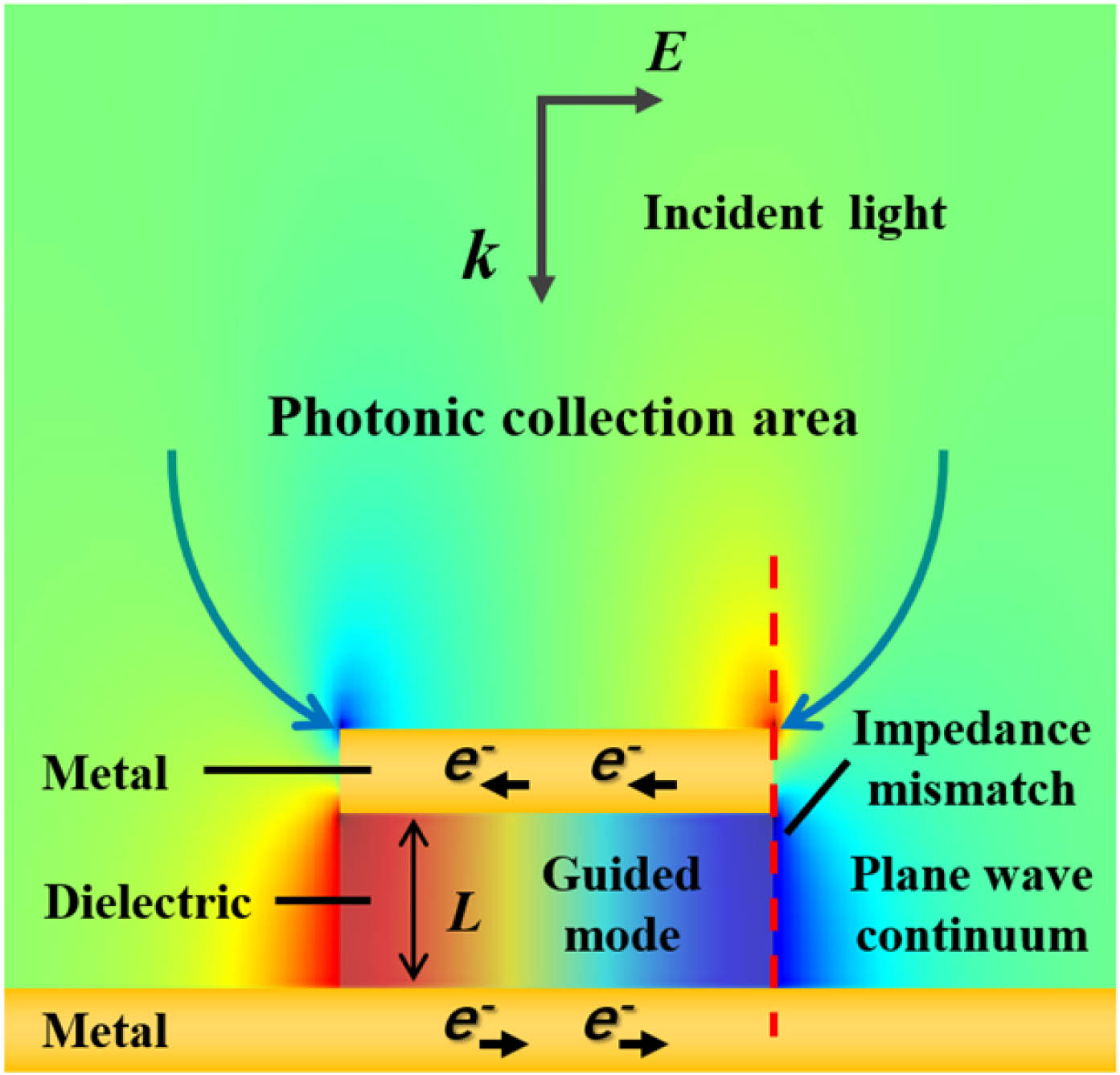
    Figure 1.Illustration of a patch antenna. The figure shows the simulated vertical component of the distribution of the electric field Ez in the dielectric area. The impedance mismatch between the single-metal and double-metal regions leads to a lateral Fabry–Perot effect and hence the formation of the standing wave pattern.

    The device architecture and material energy band diagram are described in Fig. 2. As shown in Fig. 2(a), to separate the two channels, two arrays of metal–dielectric–metal microcavity patches, which provide a strong subwavelength electric field confinement and act as antennas, are nested within each other, and respectively connected to their own top metal electrode (B and C). They share the Ti/Au ground plane as the bottom metal electrode (D). Each array consists of 20×20 periodic square patches, which are row selected electrically connected by 200-nm-wide connecting wires in the diagonal direction. The patch sizes of the arrays were designed to match the target dual-band wavelengths. According to Eq. (2), the array with patch size s1=1.5  μm is therefore in resonance with λ1=10.0  μm, while the array with patch size s2=0.9  μm is in resonance with λ2=5.7  μm. As long as the dielectric layer thickness L is small enough, the detection wavelengths of the patch-antenna array are determined by their patch sizes only, and are independent with the period p. However, p affects the absorption efficiency of the device, which is related to the effective optical area of the patch antenna. In this work, the period p of both arrays was chosen to be 5 μm, in the same order of magnitude as the target detection wavelengths. By separately reading out the electrical signals between the metal electrodes B-D, C-D, and BC-D, the operating mode can be freely switched among long-wave, mid-wave, and dual-color.

    (a) Scanning electron microscope image of the detector, with partial enlargements of the electrically connected patch antennas. The main parameters of the array are indicated in the diagram. Region A: the photonic collection area. Region B: the top metal electrode for the 10.0-μm channel. Region C: the top metal electrode for the 5.7-μm channel. Region D: the bottom metal electrode. Region E: SiO2 for electrical insulation. Region F: the Ti/Au ground plane. (b) Conduction band diagram and relevant energy levels of one period active core. The shaded wells are Si doped, and the optical transitions are indicated by the black arrows.

    Figure 2.(a) Scanning electron microscope image of the detector, with partial enlargements of the electrically connected patch antennas. The main parameters of the array are indicated in the diagram. Region A: the photonic collection area. Region B: the top metal electrode for the 10.0-μm channel. Region C: the top metal electrode for the 5.7-μm channel. Region D: the bottom metal electrode. Region E: SiO2 for electrical insulation. Region F: the Ti/Au ground plane. (b) Conduction band diagram and relevant energy levels of one period active core. The shaded wells are Si doped, and the optical transitions are indicated by the black arrows.

    To match the device design, the active region of the wafer composed of five periods of infrared dual-band quantum cascade active cores was optimized to room temperature operation. The layer sequence of one period of the structure in nanometers is as follows: 4.5, 6.7, 2.0, 3.1, 4.9, 3.25, 4.6, 3.25, 4.4, 3.4, 2.5, 3.9, 2.8, 4.9, 3.0, 6.25, where the In0.52Al0.48As barrier layers are in bold font, the In0.53Ga0.47As well layers are in normal font, and the underlined layers are Si doped to n=3×10¹⁷  cm3. The conduction band diagram and relevant energy levels of one period active core are shown in Fig. 2(b). In this design, the dual-color detection is achieved by a vertical transition in the active quantum well (E0ET) and a diagonal transition across the adjacent quantum wells (E0Emini).

    Taking account of the actual situation with connecting wires, the simulated electric field component distribution and reflectivity spectrum are presented in Fig. 3. Since the patch connecting wires lead to the asymmetry of the geometry, the incident light with different polarization directions was investigated. For the sake of convenience, the direction perpendicular to the connecting wires is specified as the 0° polarization direction. Since both natural light and circularly polarized light can be regarded as the synthesis of two linearly polarized lights with equal amplitude and vertical vibration direction, circularly polarized incidence was used instead of natural incidence in this simulation. Figure 3(a) indicates that the patch antennas with different sizes have strong coupling effects on the light with specific wavelengths. In addition, when the polarization direction of the incident light is perpendicular to the connecting wires, the electric field distribution follows a standing wave pattern, with the node at the center of the square and the antinode at the edges, showing strong field localization in the dielectric region. When the polarization direction of the incident light is parallel to the connecting wires, the electric field distribution is disturbed.

    (a) Respectively normalized simulated distribution of the absolute vertical component of the electric field |Ez| at the center plane of the active region. The wavelengths and polarization directions of the incident light are indicated in the figure. (b) Simulated reflectivity spectrum of the devices.

    Figure 3.(a) Respectively normalized simulated distribution of the absolute vertical component of the electric field |Ez| at the center plane of the active region. The wavelengths and polarization directions of the incident light are indicated in the figure. (b) Simulated reflectivity spectrum of the devices.

    As shown in Fig. 3(b), the reflectivity dips observable in the spectra correspond to resonant absorption within the structure. When Eq. (1) is satisfied, the incident photons are coupled into the structure, yielding the reflectivity minima in the spectra. While p=5  μm, the reflectivity of the array reached nearly 0 at the target resonant wavelengths. The existence of the connecting wires in the polarization direction of the incident light leads to a decrease of the absorption intensity and a shift of the peak absorption wavelength. Inspired by the polarization dependence of this design, it is suggested that the cross talk between two channels can be reduced by modulating the polarization direction of the incident light, which is confirmed by the subsequent results.

    3. CHARACTERIZATION AND ANALYSIS

    The detector chip was mounted on an oxygen-free copper heat sink and fixed on the cold finger of a well-designed liquid-nitrogen cryostat to perform device characterization. The optical characterization of the device at zero bias was obtained with a Fourier transform infrared spectrometer and calibrated with a 1000°C blackbody source. Figure 4(a) presents the normalized responsivity spectrum of the device at 77 K and zero bias, in the case of unpolarized incident light. The operating mode of the device can be freely switched among mid-wave, long-wave, and dual-color. The two response peaks are centered at 5.7 μm (218 meV) and 10.0 μm (124 meV), respectively. The peak responsivity Rpeak of the detector as a function of the temperature at zero bias is shown in Fig. 4(b), and the Johnson noise-limited detectivity obtained according to the formula DJ*=RpeakR0A4kBT is shown in Fig. 4(c), where R0 is the differential resistance at zero bias, A is the area of the detector, kB is the Boltzmann constant, and T is the operating temperature of the detector. As the temperature increased gradually from 77 K, the responsivity slightly increased initially and subsequently decreased, which is ascribed to the inefficient ionization of the donor dopants at the liquid nitrogen temperature [35]. Nevertheless, the Johnson noise-limited detectivity continued to decrease with the increasing temperature, as the value of R0A decreased much faster than that of Rpeak increased. The operating temperature has reached room temperature when the device works in the dual-color mode or the long-wave mode, and a near-room temperature of 280 K when the device works in the mid-wave mode. At 77 K, the 5.7-μm channel achieved a peak responsivity of 34.6 mA/W and exhibited a detectivity of 2.0×10¹⁰ Jones, while the 10.0-μm channel achieved a peak responsivity of 87.5 mA/W, giving a detectivity of 5.0×10¹⁰ Jones. At the dual-color operating mode, the ratio of the peak responsivity of the 5.7-μm channel and the 10.0-μm channel was 1:2.5.

    (a) Normalized responsivity spectrum of the device at 77 K and zero bias, in the case of unpolarized incident light. (b) Peak responsivity of the device as a function of temperature. (c) Detectivity of the device as a function of temperature. From left to right, the device works in dual-color, long-wave, and mid-wave modes sequentially.

    Figure 4.(a) Normalized responsivity spectrum of the device at 77 K and zero bias, in the case of unpolarized incident light. (b) Peak responsivity of the device as a function of temperature. (c) Detectivity of the device as a function of temperature. From left to right, the device works in dual-color, long-wave, and mid-wave modes sequentially.

    While the detector operated in single-color master mode, the corresponding slave wavelength was not thoroughly filtered out, resulting in cross talk. For simplicity, the cross talk of narrowband dual-color detection can be defined as the peak responsivity ratio of the slave to master detection bands. The cross talk of the mid-wave and the long-wave operating mode was 1:12.4 and 1:5.7, respectively. The reason for the cross talk is that the active region itself can respond to two wavelengths simultaneously, as long as the ISB selection rule is fulfilled. Since the bottom Ti/Au ground plane has a scattering effect on the incident light, the scattered light is not perpendicular to the quantum well layers. This effect leads to an electric field vector component perpendicular to the quantum well layers, and results in the response of the slave detection band. Interestingly, the long-wave signal was easier to be filtered out although its peak responsivity was higher than that of the mid-wave signal. This is mainly because the dimensions of the patch antennas and the incident light are of the same order of magnitude. So there exists diffraction effect, which is closely related to the ratio of the slave detection wavelength λ and the size s (r=λ/s). The larger the ratio is, the more obvious the diffraction effect is, and the less radiation enters the active region. This ratio when the device works in the mid-wave mode (r=11.1) is much larger than that when the device works in the long-wave mode (r=3.8), and that is why the long-wave signal was easier to be filtered out.

    As mentioned above, the polarization dependence helps to lower the cross talk for these kinds of patches with antisymmetric structure. To decrease the cross talk, polarization modulation was introduced to the incident light. Through setting a polarizer in front of the optical window of the cryostat, the polarization angle of the incident light can be modulated. The normalized responsivity spectrum of the detector as a function of the polarization angle of the incident light, at 77 K and zero bias, is shown in Fig. 5(a). The ratio of the responsivity between the two detection wavelengths varies with the polarization angle, but the shift of the peak position is almost negligible. As the polarization angle increases from 0° to 90°, the FWHM of the spectra also increases, which is attributed to the gradual decrease of standing wave effect with the increase of polarization angle under this integrated patch connecting wires condition. Figure 5(b) presents the peak responsivity of the two detection wavelengths as a function of the polarization angle. For the 5.7-μm channel, the peak responsivity reached the maximum value of 20.3 mA/W at 0° polarization angle, and the minimum of 9.4 mA/W at 90° polarization angle. For the 10.0-μm channel, the peak responsivity reached the maximum value of 78.8 mA/W at 0° polarization angle, and the minimum of 47.3 mA/W at 90° polarization angle.

    (a) Normalized responsivity spectrum of the detector as a function of the polarization angle of the incident light, at 77 K and zero bias. (b) Peak responsivity as a function of the polarization angle, at 77 K and zero bias. From left to right, the device works in dual-color, long-wave, and mid-wave modes, respectively.

    Figure 5.(a) Normalized responsivity spectrum of the detector as a function of the polarization angle of the incident light, at 77 K and zero bias. (b) Peak responsivity as a function of the polarization angle, at 77 K and zero bias. From left to right, the device works in dual-color, long-wave, and mid-wave modes, respectively.

    The ratio of the responsivity of the two channels as a function of the polarization angle is shown in Fig. 6. The black dotted line reflects the ratio of the peak responsivity of the two channels when the device works in the dual-color mode, while the blue and red dotted lines reflect the cross talk when the device works in the single-color mode. Since the angles between the polarizer and the patch-antenna array were measured inaccurately, the experimental data seem to be asymmetrical with respect to the 0° polarization angle. However, according to the geometric symmetry of the device, it can be deduced that the responsivities as a function of the polarization angle were in fact symmetrical. Then we can see that the cross talk reaches the minimum at 90° for both the 5.7-μm channel and the 10.0-μm channel, being reduced to 1:22.5 and 1:7.6, respectively. At 0° polarization angle, the corresponding values are 1:8.6 and 1:5.0, respectively. The polarization angle with minimal cross talk for both channels is consistent with each other, which facilitates practical applications. Although the responsivity is also the minimum at that time as shown above, for application scenarios that require lower cross talk and do not demand very high responsivity, polarization modulation can be used. In the future, through careful design, we can make the responsivity maximal and the cross talk minimal in the same polarization direction, to further improve the performance of the device.

    Ratio of the peak responsivity of the two channels as a function of the polarization angle.

    Figure 6.Ratio of the peak responsivity of the two channels as a function of the polarization angle.

    4. CONCLUSION

    In summary, we have reported the concept demonstration of an antenna-enhanced dual-color quantum cascade detector with freely switched operating modes among mid-wave, long-wave, and dual-color. At 77 K, the 5.7-μm channel achieved a peak responsivity of 34.6 mA/W and exhibited a detectivity of 2.0×10¹⁰ Jones, while the 10.0-μm channel achieved a peak responsivity of 87.5 mA/W, giving a detectivity of 5.0×10¹⁰ Jones. The cross talk of the mid-wave and the long-wave operating modes was 1:12.4 and 1:5.7, respectively. By modulating the polarization angle of the incident light, the cross talk reached the minimum at 90° for both the 5.7-μm channel and the 10.0-μm channel, and was 1:22.5 and 1:7.6, respectively. Such an all-in-one device also shows potential of working as single- or dual-color photodetectors at room temperature. This work has proposed a novel approach in making multicolor infrared imagers and for the first time, successfully realized the signals of two channels output independently as well as simultaneously.

    Acknowledgment

    Acknowledgment. The authors would like to thank Ping Liang and Ying Hu for their help in device processing.

    APPENDIX A: CONTROL DEVICE WITH CONNECTING WIRES PARALLEL TO THE EDGE OF THE PATCH ANTENNA

    As a control experiment, we have also designed and fabricated a patch-antenna-array device, with connecting wires parallel to the edge of the patch antenna, as shown in Fig. 7. For the sake of convenience, we name the device mentioned in the main text “Patch-Diagonal,” and the control device “Patch-Parallel,” respectively. And the experimental results are shown in Figs. 8 and 9.

    Partial enlargement of the electrically connected patch antennas of the “Patch-Parallel” device.

    Figure 7.Partial enlargement of the electrically connected patch antennas of the “Patch-Parallel” device.

    Peak responsivity of the “Patch-Parallel” device as a function of the polarization angle, at 77 K and zero bias. From left to right, the device works in dual-color, long-wave, and mid-wave modes, respectively.

    Figure 8.Peak responsivity of the “Patch-Parallel” device as a function of the polarization angle, at 77 K and zero bias. From left to right, the device works in dual-color, long-wave, and mid-wave modes, respectively.

    Ratio of the peak responsivity of the “Patch-Parallel” device of the two channels as a function of the polarization angle.

    Figure 9.Ratio of the peak responsivity of the “Patch-Parallel” device of the two channels as a function of the polarization angle.

    It is illustrated that both the “Patch-Diagonal” and “Patch-Parallel” devices are mode-switchable, and the cross talk can be reduced by polarization modulation. However, for the “Patch-Parallel” device, the polarization directions with the lowest cross talk for the two channels are inconsistent due to the difference in relative size of the connection line and the mesa, which is unfavorable to the practical applications. For the “Patch-Diagonal” device as above mentioned, these two directions are consistent.

    References

    [1] A. Rogalski, J. Antoszewski, L. Faraone. Third-generation infrared photodetector arrays. J. Appl. Phys., 105, 091101(2009).

    [2] A. Rogalski. Recent progress in infrared detector technologies. Infrared Phys. Technol., 54, 136-154(2011).

    [3] J. A. Montoya, Z.-B. Tian, S. Krishna. Ultra-thin infrared metamaterial detector for multicolor imaging applications. Opt. Express, 25, 23343-23355(2017).

    [4] S. Krishna. The infrared retina. J. Phys. D, 42, 234005(2009).

    [5] L. G. A. Mark, I. C. Chein. Chemical vapor detection with a multispectral thermal imager. Opt. Eng., 30, 1725-1733(1991).

    [6] S. D. Gunapala, S. V. Bandara, J. K. Liu. Towards dualband megapixel QWIP focal plane arrays. Infrared Phys. Technol., 50, 217-226(2007).

    [7] L. Gendron, C. Koeniguer, X. Marcadet. Quantum cascade detectors. Infrared Phys. Technol., 47, 175-181(2005).

    [8] P. Reininger, B. Schwarz, H. Detz. Diagonal-transition quantum cascade detector. Appl. Phys. Lett., 105, 091108(2014).

    [9] S. Sakr, E. Giraud, A. Dussaigne. Two-color GaN/AlGaN quantum cascade detector at short infrared wavelengths of 1 and 1.7  μm. Appl. Phys. Lett., 100, 181103(2012).

    [10] L. Li, D. Xiong, J. Wen. A surface plasmonic coupled mid-long-infrared two-color quantum cascade detector. Infrared Phys. Technol., 79, 45-49(2016).

    [11] L. Li, H. Chen, Z. Fang. An electrically modulated single-color/dual-color imaging photodetector. Adv. Mater., 32, 1907257(2020).

    [12] A. M. Hoang, A. Dehzangi, S. Adhikary. High performance bias-selectable three-color short-wave/mid-wave/long-wave infrared photodetectors based on type-II InAs/GaSb/AlSb superlattices. Sci. Rep., 6, 24144(2016).

    [13] X. Wang, J. Liu, S. Zhai. Room temperature quantum cascade detector operating at 4.3  μm. J. Semicond., 35, 104009(2014).

    [14] K. Guo, Y.-X. Zhu, K. Li. Very long wave infrared quantum cascade detector with a twin-well absorption region. Appl. Phys. Lett., 121, 061101(2022).

    [15] B. Schwarz, P. Reininger, A. Harrer. The limit of quantum cascade detectors: a single period device. Appl. Phys. Lett., 111, 061107(2017).

    [16] Y. C. Wang, S. S. Li. Design of a two-dimensional square mesh metal grating coupler for a miniband transport GaAs quantum-well infrared photodetector. J. Appl. Phys., 75, 582-587(1994).

    [17] D. Hofstetter, M. Graf, T. Aellen. 23  GHz operation of a room temperature photovoltaic quantum cascade detector at 5.35  μm. Appl. Phys. Lett., 89, 061119(2006).

    [18] F. R. Giorgetta, E. Baumann, R. Théron. Short wavelength (4  μm) quantum cascade detector based on strain compensated InGaAs/InAlAs. Appl. Phys. Lett., 92, 121101(2008).

    [19] S.-Q. Zhai, J.-Q. Liu, F.-Q. Liu. A normal incident quantum cascade detector enhanced by surface plasmons. Appl. Phys. Lett., 100, 181104(2012).

    [20] G. Ariyawansa, M. B. M. Rinzan, M. Alevli. GaN/AlGaN ultraviolet/infrared dual-band detector. Appl. Phys. Lett., 89, 091113(2006).

    [21] D.-W. Jiang, W. Xiang, F.-Y. Guo. Low crosstalk three-color infrared detector by controlling the minority carriers type of InAs/GaSb superlattices for middle-long and very-long wavelength. Chin. Phys. Lett., 33, 048502(2016).

    [22] S. D. Gunapala, S. V. Bandara, J. K. Liu. Demonstration of megapixel dual-band QWIP focal plane array. IEEE J. Quantum Electron., 46, 285-293(2010).

    [23] Y. Nga Chen, Y. Todorov, B. Askenazi. Antenna-coupled microcavities for enhanced infrared photo-detection. Appl. Phys. Lett., 104, 031113(2014).

    [24] D. Palaferri, Y. Todorov, A. Bigioli. Room-temperature nine-μm-wavelength photodetectors and GHz-frequency heterodyne receivers. Nature, 556, 85-88(2018).

    [25] M. Hakl, Q. Lin, S. Lepillet. Ultrafast quantum-well photodetectors operating at 10  μm with a flat frequency response up to 70  GHz at room temperature. ACS Photonics, 8, 464-471(2021).

    [26] G. Quinchard, C. Mismer, M. Hakl. High speed, antenna-enhanced 10.3  μm quantum cascade detector. Appl. Phys. Lett., 120, 091108(2022).

    [27] D. Palaferri, Y. Todorov, Y. N. Chen. Patch antenna terahertz photodetectors. Appl. Phys. Lett., 106, 161102(2015).

    [28] D. Palaferri, Y. Todorov, A. Mottaghizadeh. Ultra-subwavelength resonators for high temperature high performance quantum detectors. New J. Phys., 18, 113016(2016).

    [29] Y. Zhu, S. Zhai, J. Liu. Mid-wave/long-wave dual-color infrared quantum cascade detector enhanced by antenna-coupled microcavity. Opt. Express, 29, 37327-37335(2021).

    [30] W. L. Barnes, A. Dereux, T. W. Ebbesen. Surface plasmon subwavelength optics. Nature, 424, 824-830(2003).

    [31] H. Liu, P. Lalanne. Microscopic theory of the extraordinary optical transmission. Nature, 452, 728-731(2008).

    [32] H. T. Miyazaki, Y. Kurokawa. Squeezing visible light waves into a 3-nm-thick and 55-nm-long plasmon cavity. Phys. Rev. Lett., 96, 097401(2006).

    [33] Y. Todorov, L. Tosetto, J. Teissier. Optical properties of metal-dielectric-metal microcavities in the THz frequency range. Opt. Express, 18, 13886-13907(2010).

    [34] C. Feuillet-Palma, Y. Todorov, A. Vasanelli. Strong near field enhancement in THz nano-antenna arrays. Sci. Rep., 3, 1361(2013).

    [35] K. Li, F. Ren, S.-M. Liu. High responsivity quantum cascade detectors with bound-to-miniband diagonal transition. Appl. Phys. Lett., 119, 051101(2021).

    Yixuan Zhu, Shenqiang Zhai, Kun Li, Kai Guo, Qiangqiang Guo, Jinchuan Zhang, Shuman Liu, Lijun Wang, Fengqi Liu, Junqi Liu. Mode-switchable dual-color infrared quantum cascade detector[J]. Photonics Research, 2024, 12(2): 253
    Download Citation