
Mao Yanjie, Li Sikun, Wang Xiangzhao, Wei Yayi, Chen Guodong. Multi-Parameter Joint Optimization for Lithography Based on Photoresist Topography Model[J]. Acta Optica Sinica, 2020, 40(4): 422002
- Acta Optica Sinica
- Vol. 40, Issue 4, 422002 (2020)
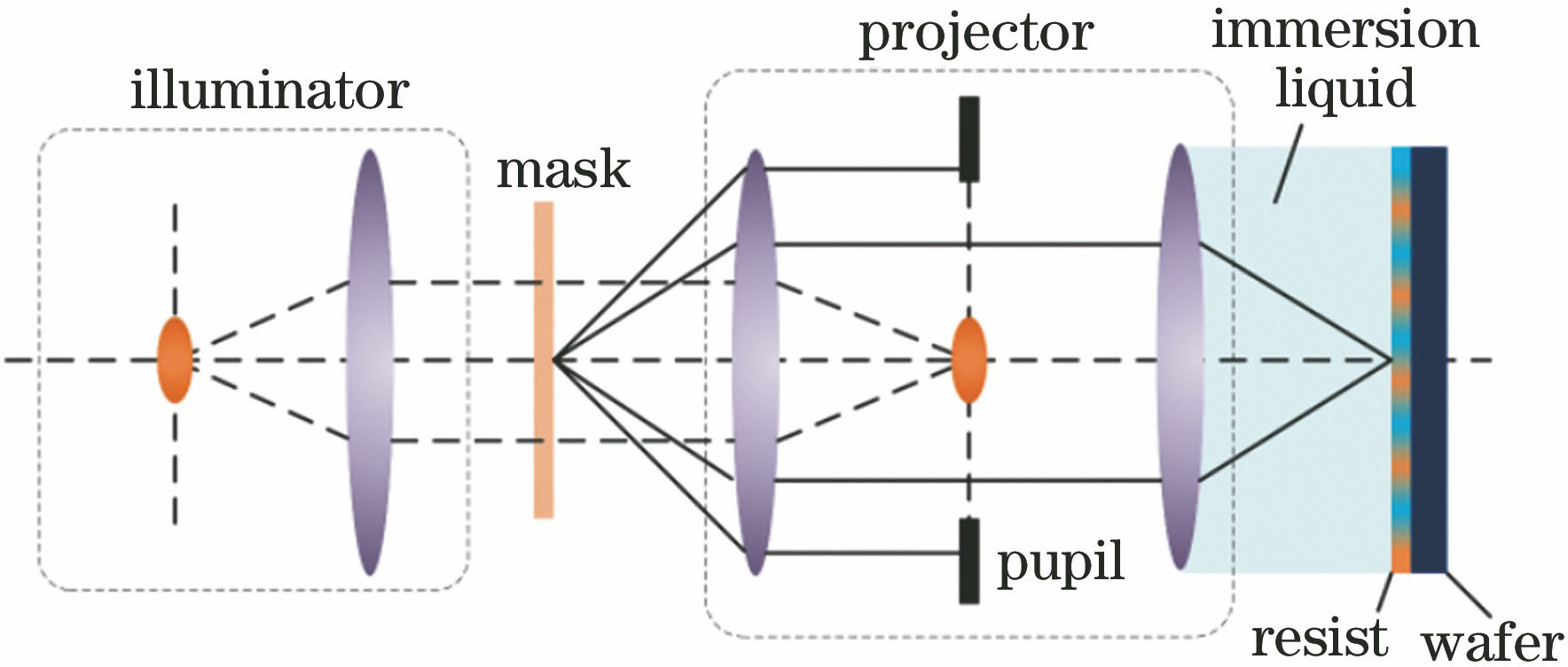
Fig. 1. Schematic of lithographic projection system
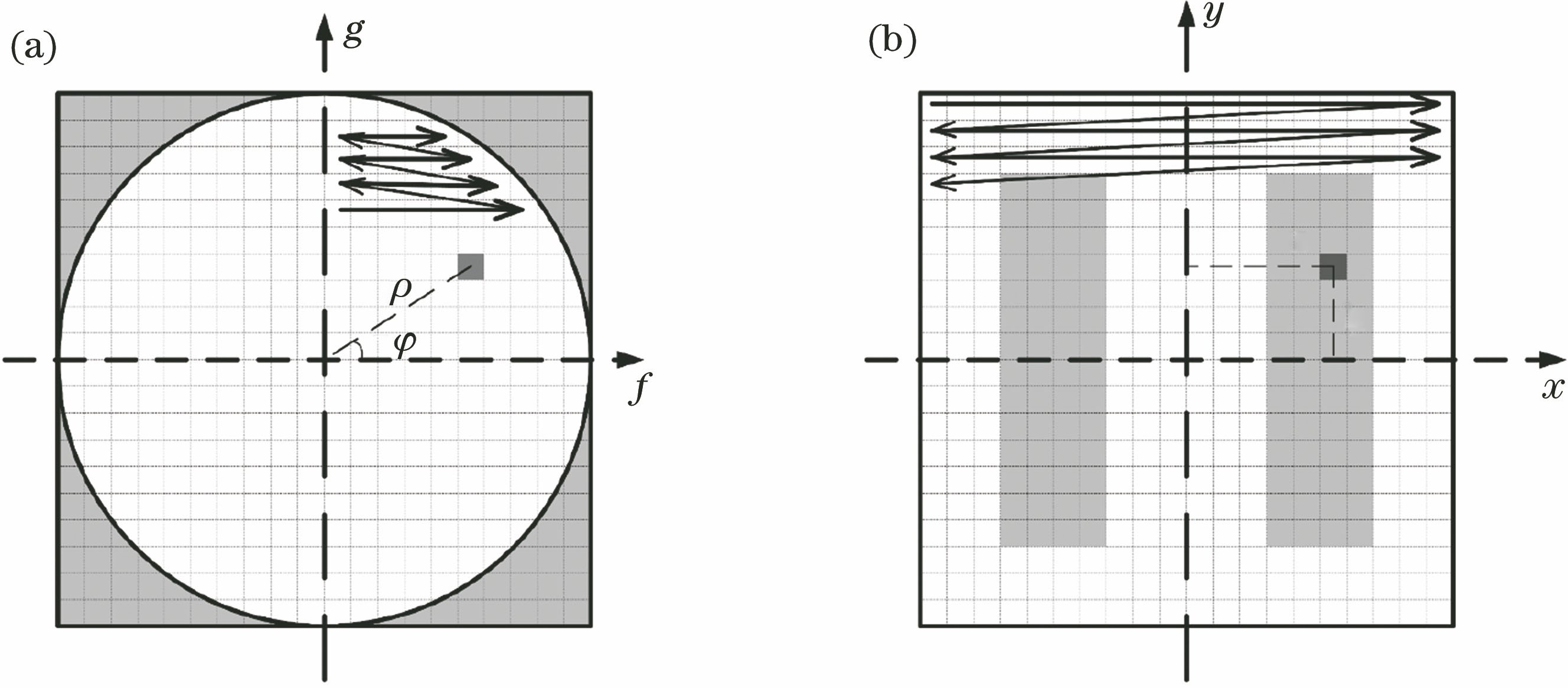
Fig. 2. Coding scheme of source and mask. (a) Coding scheme of source; (b) coding scheme of mask
Fig. 3. Illustration of the JADE mutation strategy
Fig. 4. Workflow of proposed method. (a) General flow chart; (b) source or mask optimization; (c) selection operation; (d) evaluation function calculation
Fig. 5. Initial status of objects to be optimized. (a) Mask; (b) source; (c) projector pupil
Fig. 6. Mask, source and projector pupil after optimization by proposed method. (a) Mask; (b) source; (c) projector pupil
Fig. 7. Mask, source, and projector pupil after optimization by SMPO-AI. (a) Mask; (b) source; (c) projector pupil
Fig. 8. Intensity distributions on photoresist top surface. (a) Before optimization; (b) after optimization by SMPO-AI; (c) after optimization by proposed method
Fig. 9. Surface profiles of photoresist. (a) Before optimization; (b) after optimization by SMPO-AI; (c) after optimization by proposed method
Fig. 10. Sectional profiles of photoresist. (a) Before optimization; (b) after optimization by SMPO-AI; (c) after optimization by proposed method
Fig. 11. Convergence curves of two methods. (a) SMPO-AI; (b) proposed method
Fig. 12. Convergence curves of two methods
Fig. 13. Process window before and after optimization. (a) Process window; (b) exposure latitude versus depth of focus
Fig. 14. Optimization results of complex pattern. (a) Target pattern; (b) optimized mask; (c) optimized source; profiles of photoresist (d) before optimization and (e) after optimization; (f) optimized projector pupil
Fig. 15. Sectional diagrams of photoresist morphology before and after optimization of complex pattern. (a) Before optimization; (b) after optimization
Fig. 16. Photoresist morphology after optimization of complex pattern
Fig. 17. Process window after optimization of complex pattern. (a) Process window; (b) exposure latitude versus depth of focus
Fig. 18. Optimization results of SRAM pattern. (a) Target pattern; (b) optimized mask; (c) optimized source; profiles of photoresist (d) before optimization and (e) after optimization; (f) optimized projector pupil
Fig. 19. Process window after optimization of SRAM pattern. (a) Process window; (b) exposure latitude versus depth of focus
|
Table 1. Photoresist stack data
| |||||||||||||||||||||||||||
Table 2. Process window before and after optimization

Set citation alerts for the article
Please enter your email address
© Copyright 2018-2021 | Chinese Laser Press. All Rights Reserved 沪ICP备15018463号-20