• Journal of Semiconductors
  • Vol. 40, Issue 1, 012801 (2019)
Tsung-Han Yang, Houqiang Fu, Hong Chen, Xuanqi Huang, Jossue Montes, Izak Baranowski, Kai Fu, and Yuji Zhao
Author Affiliations
  • School of Electrical, Computer and Energy Engineering, Arizona State University, Tempe, AZ 85287, USA
  • show less
    DOI: 10.1088/1674-4926/40/1/012801 Cite this Article
    Tsung-Han Yang, Houqiang Fu, Hong Chen, Xuanqi Huang, Jossue Montes, Izak Baranowski, Kai Fu, Yuji Zhao. Temperature-dependent electrical properties of β-Ga2O3 Schottky barrier diodes on highly doped single-crystal substrates[J]. Journal of Semiconductors, 2019, 40(1): 012801 Copy Citation Text show less

    Abstract

    Beta-phase gallium oxide (β-Ga2O3) Schottky barrier diodes were fabricated on highly doped single-crystal substrates, where their temperature-dependent electrical properties were comprehensively investigated by forward and reverse current density – voltage and capacitance – voltage characterization. Both the Schottky barrier height and the ideality factor showed a temperature-dependence behavior, revealing the inhomogeneous nature of the Schottky barrier interface caused by the interfacial defects. With a voltage-dependent Schottky barrier incorporated into thermionic emission theory, the inhomogeneous barrier model can be further examined. Furthermore, the reverse leakage current was found to be dominated by the bulk leakage currents due to the good material and surface quality. Leakage current per distance was also obtained. These results can serve as important references for designing efficient β-Ga2O3 electronic and optoelectronic devices on highly doped substrates or epitaxial layers.

    1. Introduction

    III-oxide compound semiconductors hold great potential to pioneer new semiconductor-based technologies. This material system, including gallium oxide (Ga2O3) and aluminum oxide (Al2O3), has a bandgap range of 4–8 eV which is much larger than that of conventional semiconductors such as silicon (1.12 eV) and gallium arsenide (1.42 eV) and even wider bandgap (WBG) semiconductors such as GaN (3.4 eV) and 4H-SiC (3.25 eV). Among these III-oxide semiconductors, beta-phase Ga2O3 (β-Ga2O3) has garnered considerable attention for various optoelectronic and electronic applications[1, 2], due to its large bandgap (~4.8 eV) and high breakdown electric field Ebr (~8 MV/cm)[35]. The large bandgap of β-phase Ga2O3 allows it to withstand a stronger electric field, which makes it possible to use a thinner device for a given voltage rating. This is important because the thinner the device, the lower its on-resistance, thus making it much more energy-efficient. As a result, β-Ga2O3 based devices are promising candidates for efficient power conversion[6, 7] application in smart grids, renewable energy, big data center power supplies, and automotive electronics.

    Another advantage of β-Ga2O3 is the availability of cost-effective single-crystal substrates[4, 8, 9]. The edge-defined film-fed growth (EFG) method, described by Labelle and Mlavsky, is an advantageous technique for growing crystals of various materials in various shapes. The EFG method has been applied to the growth of oxides such as Al2O3, LiNbO3, and TiO2. It is one of the main methods used to grow large-sized β-Ga2O3 substrates, as its relatively low cost and scalability make it well suited for use in mass production. Nowadays, commercialized high quality 2-inch β-Ga2O3 substrates grown by EFG with controllable doping concentrations ranging from 1016 to 1019 cm−3 have also been demonstrated[810]. Electronic devices such as field effect transistors (FETs)[6, 7] and Schottky barrier diodes (SBDs)[4, 8, 9, 11], and optoelectronic devices such as solar-blind photodetectors[12] fabricated on the β-Ga2O3 substrates have also been reported.

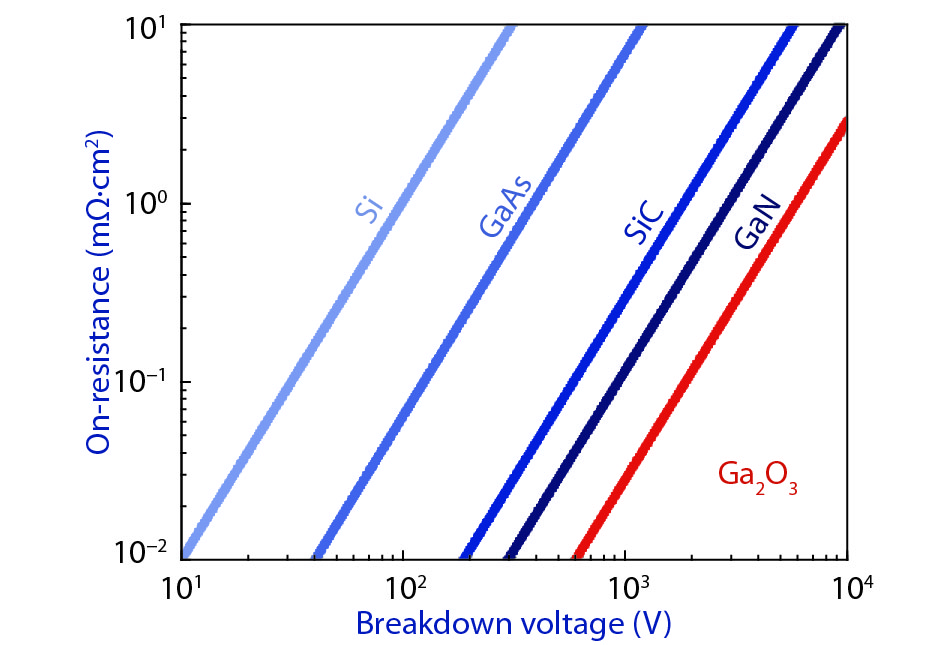
    As shown in Fig. 1, β-Ga2O3 devices are capable of dramatically enhancing the efficiency of power electronics system by reducing the on-resistance. To access this low on-resistance region, high doping concentrations of β-Ga2O3 are needed. Currently, the majority of the β-Ga2O3 devices have a doping concentration below mid 1017 cm−3 range and the on-resistance is significantly higher than the theoretical limit[3, 4], resulting in large power losses. However, there are very few reports about SBDs on highly doped single-crystal β-Ga2O3 substrates with doping concentrations above 1018 cm−3. Additionally, the mechanism of temperature-dependent performance of these SBDs is still not very clear. In this work, we comprehensively investigated the temperature-dependent electrical properties of ( ) β-Ga2O3 SBDs on highly doped (~3 × 1018 cm−3) single-crystal substrates. In Section 2, we perform detailed material characterizations on the substrates and fabricated the devices. In Section 3, first, current density–voltage (J–V) and capacitance–voltage (C–V) characteristics are discussed in detail. Several important device parameters such as Schottky barrier height and ideality factor are extracted and temperature-dependent characteristics are also included. Then, the reverse leakage currents are fitted by the trap-assisted tunneling model and the one-dimensional variable-range-hopping conduction (1D-VRH) model. Quantitative study of the leakage current as a function of distance was also carried out. These results represent one of first comprehensive investigations for β-Ga2O3 devices on highly doped substrates and are beneficial for future developments of low-loss β-Ga2O3 electronics and optoelectronics.

    (Color online) Theoretical benchmark plot of on-resistance versus breakdown voltage for power devices based on β-Ga2O3 and other major semiconductors.

    Figure 1.(Color online) Theoretical benchmark plot of on-resistance versus breakdown voltage for power devices based on β-Ga2O3 and other major semiconductors.

    2. Material characterization and device fabrication

    The β-Ga2O3 single crystal substrates were purchased from the Tamura Corporation. The wafers were grown by the EFG method. Ga2O3 and tin oxide (SnO2) powder were used as the source material and the precursor for n-type Sn dopants, respectively. More details about the growth process can be found elsewhere[9]. High-resolution X-ray diffraction (HRXRD) was used to characterize the crystal quality of the substrate. The setup was the PANalytical X’Pert Pro materials research X-ray diffractometer (MRD) system using a Cu Kα1 radiation source with a wavelength of 1.541 Å. The incident beam optics and the diffracted beam optics were the hybrid monochromator and the triple axis module, respectively. The rocking curve (RC) for the ( 01) β-Ga2O3 substrate is shown in Fig. 2(a). The full width at half maximum (FWHM) of the RC was ~44 arc sec. The dislocation density of the substrate was estimated to be of the order of ~106 cm−2[13]. To further confirm the quality of the substrate, the surface roughness was examined by using Bruker's Multimode atomic force microscopy (AFM) as shown in Fig. 2(b). The root-mean-square (RMS) roughness of the scanning area of 3 × 3 μm2 is about 0.12 nm. The HRXRD and AFM results indicate that the β-Ga2O3 substrate has a low dislocation density and a good surface morphology.

    The SBDs were then fabricated on the β-Ga2O3 substrate using standard photolithography. Before the metal depositions, the sample was cleaned in acetone and isopropyl alcohol (IPA) under ultrasonic to remove possible organic contaminants on the surface. For the ohmic contacts of the SBDs, Ti/Al/Ti/Au metal stacks were deposited on the Ga2O3 substrate using electron beam evaporation and subsequently annealed at 470 °C for 1 min in nitrogen ambient using rapid thermal annealing (RTA). For the Schottky contacts, Pt/Au metal stacks were deposited by electron beam evaporation. Fig. 2(c) shows the schematic top view and cross-section view of the β-Ga2O3 SBDs. The diameters of the left ohmic contact and right Schottky contact are 400 and 200 μm, respectively. The distance between the ohmic and Schottky contacts varied from 50 to 500 μm. A Keithley 2410 source meter and 4200-SCS parameter analyzer on a probe station with a controllable thermal chuck were used for the electrical measurement.

    (Color online) (a) The rocking curve of the β-Ga2O3 substrates measured by HRXRD. (b) The 2D and 3D AFM images of the surface morphology of the β-Ga2O3 substrates. (c) Top and cross-section view of the fabricated SBDs.

    Figure 2.(Color online) (a) The rocking curve of the β-Ga2O3 substrates measured by HRXRD. (b) The 2D and 3D AFM images of the surface morphology of the β-Ga2O3 substrates. (c) Top and cross-section view of the fabricated SBDs.

    3. Results and discussions

    3.1. Forward J–V characterization and C–V characterization

    Fig. 3 shows the temperature-dependent forward I–V characteristics of the β-Ga2O3 SBDs from 300 to 480 K (with steps of 20 degrees) in both linear scale and log scale. The upper current limit of the setup is 0.1 A. A high on/off ratio of ~109 was observed. To further discuss the electrical properties, on-resistance and turn-on voltage were then extracted. In Fig. 4(a), the on-resistance of the ( 01) β-Ga2O3 SBD is about 0.9 mΩ·cm2, which is lower than for previous work[4, 10, 11, 1420]. There are several factors that can influence the on-resistance such as ohmic contact, interface quality and crystalline quality[13]. In this work, the relatively low on-resistance can be attributed to the high doping concentration, which will be further discussed in the C–V measurements later. The turn-on voltage in Fig. 4(b) gradually decreased from 0.84 to 0.64 V with the temperature increasing from 300 to 480 K. This is due to the generation of the high energy electrons and/or reduced bandgap at high temperature.

    (Color online) Temperature-dependent forward J–V characteristics of β-Ga2O3 SBDs in (a) linear scale and (b) log scale.

    Figure 3.(Color online) Temperature-dependent forward J–V characteristics of β-Ga2O3 SBDs in (a) linear scale and (b) log scale.

    (Color online) (a) Comparision of on-resistance of previously reported β-Ga2O3 SBDs on various crystal orientations. (b) The turn-on voltage was obtained by linear extrapolation of the linear I–V curves.

    Figure 4.(Color online) (a) Comparision of on-resistance of previously reported β-Ga2O3 SBDs on various crystal orientations. (b) The turn-on voltage was obtained by linear extrapolation of the linear I–V curves.

    The current–voltage characteristics of the SBDs can be studied from the thermionic emission model[11]

    $J = {A^*}{T^2}\exp \left( { - \frac{{q{\phi _{{\rm{eff}}}}}}{{kT}}} \right)\left[ {\exp \left( {\frac{{qV}}{{nkT}}} \right) - 1} \right],$  (1)

    ${J_{\rm{s}}} = {A^*}{T^2}\exp \left( { - \frac{{q{\phi _{{\rm{eff}}}}}}{{kT}}} \right),$  (2)

    where J is the current density, A* is the Richardson constant (for β-Ga2O3, it is calculated to be 41.1 A/cm2K2 using an effective electron mass of 0.34m0 and the equation )[18], T is the temperature in kelvin, q is the electron charge, ϕeff is the effective Schottky barrier height, k is the Boltzmann constant, n is the ideality factor, and Js is the saturation current density. The ideality factor can be calculated as a function of temperature by applying the function[21]:

    $n = \frac{q}{{kT}}\frac{1}{{\frac{{{\rm d}\left( {{\rm{ln}}J} \right)}}{{{\rm d}V}}}}.$  (3)

    Fig. 5 shows the extracted ideality factor and the barrier height as a function of temperature. The values of n and Js are extracted from the measured J–V data in forward bias from 0.3 to 0.5 V. If the Schottky barrier is homogeneous and the thermionic emission model is valid, then the ϕeff should be temperature independent, ideality factor should be 1, and the y-intercept of ln(Js/T2) versus 1000/T graph should retrieve A*. However, the results obtained from Fig. (5) do not match this assumption. In Fig. 5(a), when the temperature is increased from 300 to 480 K, the ideality factor decreases from 1.39 to 1.13, and the Schottky barrier height increases from 0.94 to 1.10 eV. The correlation between the ideality factor and Schottky barrier height can be further observed by a well know linear relationship[22], as shown in Fig. 5(b). Moreover, the blue dashed line in Fig. 5(d) shows a fit to the Richardson plot of ln(Js/T2) versus 1000/T. The calculated A* value is about 3.28 × 10⁻³ Acm−2K−2, which is unreasonably small compared with the theoretical value. All these non-ideal results can be explained by the thermionic emission over an inhomogeneous barrier with a voltage-dependent barrier height[23]. The spatial inhomogeneities are attributed to the defects between the metal/semiconductor interface, which may be caused by a rough interface between the Schottky electrode and the semiconductor, non-uniform metallurgy, and metal grain boundaries[24, 25]. To incorporate the barrier inhomogeneity into the thermionic emission model, it is assumed that the Schottky barrier has a Gaussian distribution potential with a mean barrier height and a standard deviation σ, and the barrier is linearly dependent on voltage:

    ${\phi _{{\rm{eff}}}} = \overline {{\phi _{\rm b}}} - \frac{{q{{\rm{\sigma }}^2}}}{{2kT}},$  (4)

    $\overline {{\phi _{\rm b}}} = \overline {{\phi _{{\rm b}0}}} + \gamma V,$  (5)

    ${{\rm{\sigma }}^2} = {{\rm{\sigma }}_0}^2 - \xi V,$  (6)

    where ϕb0 and σ0 are the values at zero bias. The ideality factor thus becomes temperature-dependent and its value can exceed unity:

    ${n^{ - 1}} - 1 = - \gamma - \frac{{q\xi }}{{2kT}}.$  (7)

    Fig. 5(c) shows the linear relationship of both n−1−1 and ϕeff with respect to 1000/T. The coefficients γ and ξ represent the voltage-induced deformation of the Schottky barrier distribution. Note that γ < 0 and ξ > 0, meaning larger voltage can decrease the mean Schottky barrier height and reduce the inhomogeneity of the barrier distribution, respectively [23]. With the fitting data in Fig. 5(c), the extracted ϕb0 is 1.34 eV and the extracted σ0 is 0.14 eV. This potential fluctuation parameter is close to the values of some other reported SBDs with different materials, such as a-IGZO (0.13 eV)[24], ZnO (0.134 eV)[26], and a-ZTO (0.12 eV)[23] Schottky diodes.

    Moreover, we can then combine the modified Schottky barrier Eq. (4) into the original thermionic emission Eq. (1) and obtain the following modified thermionic emission equation:

    ${\rm{ln}}\left( {{J_{\rm s}}/{T^2}} \right) - {q^2}{\sigma _0}^2/2{k^2}{T^2} = {\rm{ln}}\left( {{A^*}} \right) - q\overline {{\phi _{{\rm{b}}0}}} /kT.$  (8)

    A modified Richardson plot using Eq. (8) is shown in the red line of Fig. 5(d). Form the fitting data (dashed line), the modified Richardson constant A* is ~41.26 Acm−2K−2 and is ~1.36 eV. These values are close to the theoretical A* value (41.1 Acm−2K−2) and the value extracted from Fig. 5(c) (1.34 eV).

    (Color online) (a) Ideality factor and Schottky barrier height as a function of temperature from 300 to 480 K. (b) Ideality factor versus Schottky barrier height. (c) Plot of effective barrier height and n−1–1 versus 1000/T with error bars. (d) Original and modified Richardson plot for β-Ga2O3 SBDs. The dashed line shows the fitting curve.

    Figure 5.(Color online) (a) Ideality factor and Schottky barrier height as a function of temperature from 300 to 480 K. (b) Ideality factor versus Schottky barrier height. (c) Plot of effective barrier height and n−1–1 versus 1000/T with error bars. (d) Original and modified Richardson plot for β-Ga2O3 SBDs. The dashed line shows the fitting curve.

    Fig. 6(a) shows the C–V characteristics of the Ga2O3 SBDs at a frequency of 1 MHz at room temperature. By plotting the 1/C2 versus V in Fig. 6(b) and extracting the slope, the doping concentration can be calculated using the following equations[11, 27]:

    (Color online) C-V characteristics for β-Ga2O3 SBDs at 1 MHz. The doping concentration of the devices was also extracted.

    Figure 6.(Color online) C-V characteristics for β-Ga2O3 SBDs at 1 MHz. The doping concentration of the devices was also extracted.

    $\frac{1}{{{C^2}}} = \frac{2}{{q{\varepsilon _0}{\varepsilon _{\rm{r}}}{N_{\rm{D}}}}}\left( {{V_{{\rm{bi}}}} - V - \frac{{kT}}{q}} \right),$  (9)

    ${N_{\rm{D}}} = \frac{{ - 2}}{{q{\varepsilon _0}{\varepsilon _{\rm{r}}}\left[ {\frac{{{\rm{d}}\left( {\frac{1}{{{C^2}}}} \right)}}{{{\rm{d}}V}}} \right]}},$  (10)

    where ε0 is vacuum permittivity, εr is the relative permittivity of β-Ga2O3, and Vbi is the built-in voltage. The doping concentration of the β-Ga2O3 substrate is about (2.9–3.5) ×1018 cm−3, which is a relatively high doping concentration. This result indicates that this sample is less resistive and explains the low on-resistance of the devices.

    3.2. Reverse J–V characterization and the study of the surface current leakage

    The temperature-dependent reverse J–V characteristics of the β-Ga2O3 SBDs is presented in Fig. 7. Note that the breakdown voltages were relatively low due to the high doping concentration of the substrates. The reverse current increased with the temperature, increasing from 300 to 480 K. Due to the ultra large bandgap of β-Ga2O3, the thermionic emission current over the barrier is very small compared to the measured current levels, hence it will be neglected in the following discussion[28]. To study the reverse leakage current mechanism, several current conduction models are proposed to characterize the reverse leakage current[2832]. The first model is the two-step trap-assisted tunneling[2830, 32]. In this model, an electron in the metal could be activated to a trap state at the metal–semiconductor interface and then tunnel to the semiconductor side. Fig. 8(a) shows a typical Arrhenius plot of the current for this model at VR = 7 V and a schematic electron transport diagram in the inset. This phenomenon can be examined from the exponential temperature dependence of the reverse current. The reverse leakage current is proportional to an exponential term to the power of –EA/kT where EA is the activation energy. From the slope of this graph, the activation energy was extracted to be 30.5 meV. Assuming thermal activation is the rate-limiting step, the trap state would be at an energy ( ) below the conduction band edge of the semiconductor.

    (Color online) Temperature-dependent reverse J–V characteristics of the β-Ga2O3 SBDs in the (a) linear scale and (b) log scale.

    Figure 7.(Color online) Temperature-dependent reverse J–V characteristics of the β-Ga2O3 SBDs in the (a) linear scale and (b) log scale.

    The second model is the one-dimensional variable-range-hopping conduction (1D-VRH) model[31]. The model describes a thermally activated current conduction from the metal into the semiconductor along the defect states associated with a threading dislocation near or below the Fermi level. In this model, the conductivity of the device is given by[28]

    ${\rm{\sigma }} = {\sigma _0}{\rm{exp}}\left[ { - {{\left( {{T_0}/T} \right)}^{0.5}}} \right],$  ()

    where T0 is a characteristic temperature. Fig. 8(b) demonstrated the relationship of measured conductivity in log scale as a function of T−0.5 from 300 to 480 K. The good fitting between experiment data and fitting data suggest that both models play important roles in the reverse leakage mechanism. Further investigations are needed to decouple the two mechanisms and identify the primary mechanism.

    (Color online) (a) Arrhenius plot of reverse leakage currents of the β-Ga2O3 SBDs with the activation energy extracted. (b) Conductivity as a function of 1/T1/2 for the β-Ga2O3 SBDs. The inset shows the electron transport in the 1D-VRH conduction model.

    Figure 8.(Color online) (a) Arrhenius plot of reverse leakage currents of the β-Ga2O3 SBDs with the activation energy extracted. (b) Conductivity as a function of 1/T1/2 for the β-Ga2O3 SBDs. The inset shows the electron transport in the 1D-VRH conduction model.

    Fig. 9 shows the leakage current for β-Ga2O3 SBDs as a function of contact distance from 50 to 500 μm at voltages of −6, −7, and −8 V. The reverse current decreased as the contact distance increased. This trend is opposite from the observation of some other material system such as AlN on sapphire[27, 33] and germanium on SOI[34]. The total leakage current is the sum of leakage currents through the bulk and the surface. For the cases of AlN and Ge on SOI, due to the poor material quality and the large amount of surfaces states, the leakage current is surface dominated via surface states. With shorter contact distance, there is less chance for the device to have a poor surface area between the contacts. As a result, the surface leakage current increases with the contact distance. In the case of β-Ga2O3 SBDs on single-crystal substrate, without the detrimental effects of poor material quality, the leakage current is dominated by the bulk. A larger contact distance results in a higher resistivity of the leakage path and a lower leakage current. With the linear fitting, the leakage currents per distance were extracted to be 0.065, 0.156, 0.361 mA/mm at −6, −7, and −8 V, respectively. At higher reverse bias, the leakage current is increased due to a higher electric field between the contacts[35].

    (Color online) Leakage current as a function of contact distance between ohmic and Schottky contacts at different reverse voltages.

    Figure 9.(Color online) Leakage current as a function of contact distance between ohmic and Schottky contacts at different reverse voltages.

    4. Conclusions

    Lateral SBDs fabricated on highly doped β-Ga2O3 substrates by the EFG method were presented. The temperature-dependent J–V and C–V characteristics were analyzed rigorously. The C–V measurement indicated a high doping concentration of (2.9–3.5) × 1018 cm−3 of the β-Ga2O3 substrate. At the forward bias under room temperature, the SBDs exhibited a good rectifying behavior. At room temperature, the devices had a turn-on voltage of ~0.84 V, an on-resistance of ~0.9 mΩ·cm2, an on/off ratio of ~109, an ideality factor of 1.39, and a Schottky barrier height of 0.94 eV, respectively. In addition, the ideality factor showed a negative temperature dependence, and the Schottky barrier height had a positive temperature dependence. This is due to the inhomogeneous Schottky barrier interface caused by defects. Using the modified thermionic emission with the inhomogeneous Schottky barrier considered, the modified Richardson constant was found to be ~41.26 Acm−2K−2 and the mean Schottky barrier height ~1.36 eV. At the reverse bias, the device showed a relatively low breakdown voltage because of its high doping concentration. Two models including the two-step trap-assisted model and 1D-VRH model were used to fit the reverse leakage currents. Both play important roles in the reverse leakage current mechanism. The leakage current had a distinctive negative distance dependence, indicating it is bulk leakage dominated.

    References

    [1] H Sun, K H Li, C G T Castanedo et al. HCl flow-induced phase change of α-, β-, and ε- Ga2O3 films grown by MOCVD. Cryst Growth Design, 18, 2370(2018).

    [2] H Sun, C G T Castanedo, K Liu et al. Valence and conduction band offsets of β-Ga2O3/AlN heterojunction. Appl Phys Lett, 111, 162105(2017).

    [3] Z Zhang, E Farzana, A Arehart et al. Deep level defects throughout the bandgap of (010) β- Ga2O3 detected by optically and thermally stimulated defect spectroscopy. Appl Phys Lett, 108, 052105(2016).

    [4] Q He, W Mu, H Dong et al. Schottky barrier diode based on β-Ga2O3 (100) single crystal substrate and its temperature-dependent electrical characteristics. Appl Phys Lett, 110, 093503(2017).

    [5] H Tippins. Optical absorption and photoconductivity in the band edge of β-Ga2O3. Phys Rev, 140, A316(1965).

    [6] M Higashiwaki, K Sasaki, A Kuramata et al. Gallium oxide (Ga2O3) metal-semiconductor field-effect transistors on single-crystal β-Ga2O3 (010) substrates. Appl Phys Lett, 100, 013504(2012).

    [7] M Higashiwaki, K Sasaki, T Kamimura et al. Depletion-mode Ga2O3 metal–oxide–semiconductor field-effect transistors on β-Ga2O3 (010) substrates and temperature dependence of their device characteristics. Appl Phys Lett, 103, 123511(2013).

    [8] T Oishi, Y Koga, K Harada et al. High-mobility β-Ga2O3 ( 01) single crystals grown by edge-defined film-fed growth method and their Schottky barrier diodes with Ni contact. Appl Phys Express, 8, 031101(2015).

    [9] A Kuramata, K Koshi, S Watanabe et al. High-quality β-Ga2O3 single crystals grown by edge-defined film-fed growth. Jpn J Appl Phys, 55, 1202A(2016).

    [10] T Oishi, K Harada, Y Koga et al. Conduction mechanism in highly doped β-Ga2O3 single crystals grown by edge-defined film-fed growth method and their Schottky barrier diodes. Jpn J Appl Phys, 55, 030305(2016).

    [11] M Higashiwaki, K Konishi, K Sasaki et al. Temperature-dependent capacitance–voltage and current–voltage characteristics of Pt/Ga2O3 (001) Schottky barrier diodes fabricated on n-Ga2O3 drift layers grown by halide vapor phase epitaxy. Appl Phys Lett, 108, 133503(2016).

    [12] S Oh, M A Mastro, M J Tadjer et al. Solar-blind metal–semiconductor–metal photodetectors based on an exfoliated β-Ga2O3 micro-flake. ECS J Solid State Sci Technol, 6, Q79(2017).

    [13] M Higashiwaki, K Sasaki, A Kuramata et al. Development of gallium oxide power devices. Phys Status Solidi A, 211, 21(2014).

    [14] K Sasaki, A. Kuramata, T Masui et al. Device-quality β-Ga2O3 epitaxial films fabricated by ozone moleular beam epitaxy. Appl Phys Express, 5, 035502(2012).

    [15] S Ahn, F Ren, L Yuan et al. Temperature-dependent characteristics of Ni/Au and Pt/Au Schottky diodes on β-Ga2O3. ECS J Solid State Sci Technol, 6, P68(2017).

    [16] K Sasaki, D Wakimoto, Q T Thieu et al. First demonstration of Ga2O3 trench MOS-type Schottky barrier diodes. IEEE Electron Device Lett, 38, 783(2017).

    [17] J Yang, S Ahn, F Ren et al. High reverse breakdown voltage Schottky rectifiers without edge termination on Ga2O3. Appl Phys Lett, 110, 192101(2017).

    [18] K Sasaki, M Higashiwaki, A Kuramata et al. Ga2O3 Schottky barrier diodes fabricated by using single-crystal β-Ga2O3 (010) substrates. IEEE Electron Device Lett, 34, 493(2013).

    [19] J Yang, S Ahn, F Ren et al. High breakdown voltage ( 01) β-Ga2O3 Schottky rectifiers. IEEE Electron Device Lett, 38, 906(2017).

    [20] B Song, A K Verma, K Nomoto et al. Vertical Ga2O3 Schottky barrier diodes on single-crystal β-Ga2O3 ( 01) substrates. Device Research Conference (DRC), 2016, 1(2016).

    [21] H Fu, X Huang, H Chen et al. Ultra-low turn-on voltage and on-resistance vertical GaN-on-GaN Schottky power diodes with high mobility double drift layers. Appl Phys Lett, 111, 152102(2017).

    [22] F Iucolano, F. Roccaforte, F Giannazzo et al. Barrier inhomogeneity and electrical properties of Pt/Ga N Shottky contacts. J Appl Phys, 102, 113701(2007).

    [23] Y Son, R L Peterson. The effects of localized tail states on charge transport mechanisms in amorphous zinc tin oxide Schottky diodes. Semicond Sci Technol, 32, 12L(2017).

    [24] D H Lee, K Nomura, T Kamiya et al. Diffusion-limited a-IGZO/Pt Schottky junction fabricated at 200 °C on a flexible substrate. IEEE Electron Device Lett, 32, 1695(2011).

    [25] J H Werner, H H Güttler. Barrier inhomogeneities at Schottky contacts. J Appl Phys, 69, 1522(1991).

    [26] H von Wenckstern, G Biehne, R A Rahman et al. Mean barrier height of Pd Schottky contacts on ZnO thin films. Appl Phys Lett, 88, 092102(2006).

    [27] H Fu, I Baranowski, X Huang et al. Demonstration of AlN Schottky barrier diodes with blocking voltage over 1 kV. IEEE Electron Device Lett, 38, 1286(2017).

    [28] E Miller, E Yu, P Waltereit et al. Analysis of reverse-bias leakage current mechanisms in GaN grown by molecular-beam epitaxy. Appl Phys Lett, 84, 535(2004).

    [29] F Padovani, R Stratton. Field and thermionic-field emission in Schottky barriers. Solid-State Electron, 9, 695(1966).

    [30] E Miller, X Dang, E Yu. Gate leakage current mechanisms in AlGaN/GaN heterostructure field-effect transistors. J Appl Phys, 88, 5951(2000).

    [31] H Iwano, S Zaima, Y Yasuda. Hopping conduction and localized states in p-Si wires formed by focused ion beam implantations. J Vac Sci Technol B, 16, 2551(1998).

    [32] W Lu, L Wang, S Gu et al. Analysis of reverse leakage current and breakdown voltage in GaN and InGaN/GaN Schottky barriers. IEEE Trans Electron Devices, 58, 1986(2011).

    [33] H Fu, X Huang, H Chen et al. Fabrication and characterization of ultra-wide bandgap AlN-based Schottky diodes on sapphire by MOCVD. IEEE J Electron Devices Soc, 5, 518(2017).

    [34] T Loh, H Nguyen, R Murthy et al. Selective epitaxial germanium on silicon-on-insulator high speed photodetectors using low-temperature ultrathin Si0.8Ge0.2 buffer. Appl Phys Lett, 91, 073503(2007).

    [35] D Yu, C Wang, B L Wehrenberg et al. Variable range hopping conduction in semiconductor nanocrystal solids. Phys Rev Lett, 92, 216802(2004).

    Tsung-Han Yang, Houqiang Fu, Hong Chen, Xuanqi Huang, Jossue Montes, Izak Baranowski, Kai Fu, Yuji Zhao. Temperature-dependent electrical properties of β-Ga2O3 Schottky barrier diodes on highly doped single-crystal substrates[J]. Journal of Semiconductors, 2019, 40(1): 012801
    Download Citation