• Matter and Radiation at Extremes
  • Vol. 6, Issue 4, 046903 (2021)
D. Calestani1、*, M. Villani1, G. Cristoforetti2, F. Brandi2, P. Koester2, L. Labate2, and L. A. Gizzi2
Author Affiliations
  • 1IMEM-CNR, Parco Area delle Scienze 37/A, 43124 Parma, Italy
  • 2ILIL, INO-CNR, Area della Ricerca CNR di Pisa, via G. Moruzzi 1, 56124 Pisa, Italy
  • show less
    DOI: 10.1063/5.0044148 Cite this Article
    D. Calestani, M. Villani, G. Cristoforetti, F. Brandi, P. Koester, L. Labate, L. A. Gizzi. Fabrication of ZnO-nanowire-coated thin-foil targets for ultra-high intensity laser interaction experiments[J]. Matter and Radiation at Extremes, 2021, 6(4): 046903 Copy Citation Text show less
    Scheme showing proton acceleration via target normal sheath acceleration (TNSA) using nanowire-coated foils as targets.
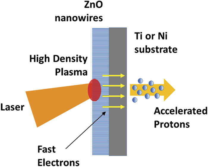
    Fig. 1. Scheme showing proton acceleration via target normal sheath acceleration (TNSA) using nanowire-coated foils as targets.
    (a) Exploded scheme showing the foil holder components. (b) Drawing of the assembled holder parts in the reaction solution.
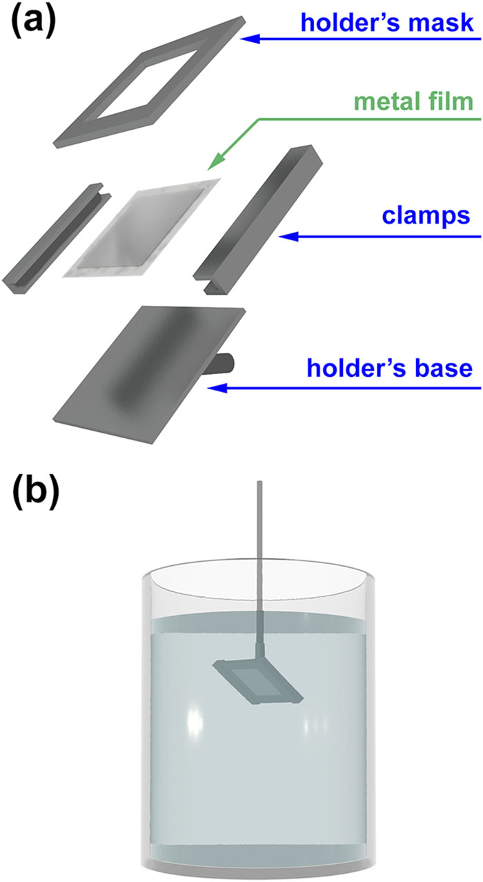
    Fig. 2. (a) Exploded scheme showing the foil holder components. (b) Drawing of the assembled holder parts in the reaction solution.
    SEM images of inhomogeneous (x) and homogenous (✓) ZnO nanowire patterns: (a) and (b) inhomogeneity in size or alignment; (c) inhomogeneity in distribution across the thin foil; (d) and (e) inhomogeneity in height or orientation due to the irregular foil surface; (f), (g), and (h) large-scale homogeneity. Images (a), (c), (f), and (g) are taken with the foil parallel to the view, while images (b), (d), (e), and (h) are taken on tilted surfaces. Image (h) is taken on an intentionally broken film to show the ZnO nanowire patterned section.
    Fig. 3. SEM images of inhomogeneous (x) and homogenous (✓) ZnO nanowire patterns: (a) and (b) inhomogeneity in size or alignment; (c) inhomogeneity in distribution across the thin foil; (d) and (e) inhomogeneity in height or orientation due to the irregular foil surface; (f), (g), and (h) large-scale homogeneity. Images (a), (c), (f), and (g) are taken with the foil parallel to the view, while images (b), (d), (e), and (h) are taken on tilted surfaces. Image (h) is taken on an intentionally broken film to show the ZnO nanowire patterned section.
    Graphic visualization of the main nanowire parameters: the nanowire length “l,” nanowire diameter “d,” nanowire-to-nanowire distance “δ,” and tilt angle “θ” with the line normal to the substrate.
    Fig. 4. Graphic visualization of the main nanowire parameters: the nanowire length “l,” nanowire diameter “d,” nanowire-to-nanowire distance “δ,” and tilt angle “θ” with the line normal to the substrate.
    SEM images of ZnO nanowires with similar diameters and different lengths. Each length is calculated via correction of image tilt.
    Fig. 5. SEM images of ZnO nanowires with similar diameters and different lengths. Each length is calculated via correction of image tilt.
    SEM images of nanostructured targets with different ZnO nanowire diameter and density ranges. Diameter ranges are labeled “THIN” for 50–150 nm, “MEDIUM” for 150–500 nm, and “HIGH” for 0.5 nm–1.5 µm. Density ranges are defined based on the ratio between the average nanowire-to-nanowire distance δ and the nanowire diameter d. Approximately δ > 5 d represents “LOW” density, 2 d < δ < 5 d represents “MEDIUM” density, and δ < 2 d represents “HIGH” density.
    Fig. 6. SEM images of nanostructured targets with different ZnO nanowire diameter and density ranges. Diameter ranges are labeled “THIN” for 50–150 nm, “MEDIUM” for 150–500 nm, and “HIGH” for 0.5 nm–1.5 µm. Density ranges are defined based on the ratio between the average nanowire-to-nanowire distance δ and the nanowire diameter d. Approximately δ > 5 d represents “LOW” density, 2 d < δ < 5 d represents “MEDIUM” density, and δ < 2 d represents “HIGH” density.
    Energy absorbed by silicon nanowire array targets with various combinations of diameter d and gaps δ-d during irradiation with a 25 fs, 800 nm laser pulse at an intensity of 5 × 10¹⁸ W/cm2. The graphs are obtained by performing 2D, fully kinetic particle-in-cell simulations using the code Aladyn.
    Fig. 7. Energy absorbed by silicon nanowire array targets with various combinations of diameter d and gaps δ-d during irradiation with a 25 fs, 800 nm laser pulse at an intensity of 5 × 10¹⁸ W/cm2. The graphs are obtained by performing 2D, fully kinetic particle-in-cell simulations using the code Aladyn.
    SEM images of ZnO nanowires with various densities and alignments: (a) a low density and alignment with a broad θ range; (b) a high density and alignment with a narrow θ range centered around 0; and (c) a nearly continuous film of extremely high density microwires.
    Fig. 8. SEM images of ZnO nanowires with various densities and alignments: (a) a low density and alignment with a broad θ range; (b) a high density and alignment with a narrow θ range centered around 0; and (c) a nearly continuous film of extremely high density microwires.
    SEM image of one of the windows in the target holder.
    Fig. 9. SEM image of one of the windows in the target holder.
    D. Calestani, M. Villani, G. Cristoforetti, F. Brandi, P. Koester, L. Labate, L. A. Gizzi. Fabrication of ZnO-nanowire-coated thin-foil targets for ultra-high intensity laser interaction experiments[J]. Matter and Radiation at Extremes, 2021, 6(4): 046903
    Download Citation