
D. Calestani, M. Villani, G. Cristoforetti, F. Brandi, P. Koester, L. Labate, L. A. Gizzi. Fabrication of ZnO-nanowire-coated thin-foil targets for ultra-high intensity laser interaction experiments[J]. Matter and Radiation at Extremes, 2021, 6(4): 046903
- Matter and Radiation at Extremes
- Vol. 6, Issue 4, 046903 (2021)
Abstract
I. INTRODUCTION
Relativistic laser interaction with matter is an exciting and promising tool for investigating the properties of matter in extreme conditions,1 reaching multi-keV temperatures at quasi-solid densities, and accelerating ions and electrons to relativistic energies. Thus, it has a multitude of potential applications. However, the energy coupling of an ultra-intense, ultra-short laser pulse with a flat target is usually quite low since the laser light is largely reflected at the plasma critical density. This results in both negligible delivery of energy (and therefore heat) to the denser regions of the plasma and inefficient conversion of laser energy into accelerated high-energy particles.
In order to circumvent this limitation, the coupling of laser energy with a target can be enhanced. This can be done in two ways: by modifying the laser pulse temporal profile to produce a smoother plasma density profile and by structuring the target surface to support laser–matter interaction. In the first scheme, a fraction of the laser light impinges on the target before the arrival of the main peak, producing a controlled μm-scale plasma in front of the solid target surface. This can be achieved by lowering the contrast of the chirped pulse amplification laser system2,3 or using laser pre-pulses emitted by the same laser system or by secondary sources. This scheme can significantly improve energy conversion into accelerated particles, increasing both their quantity and their energy. However, it requires an accurate knowledge and control of the laser pulse profile, which is often difficult to achieve. Moreover, laser absorption occurs at even larger distances from the dense plasma regions in this scheme. Thus, the dense plasma regions remain at low (less than keV) temperatures.
The second approach to improve laser-plasma coupling involves the use of targets with nano or microstructured surfaces, such as wires, tubes, gratings, and foams. Unlike in the scheme mentioned before, a high-contrast laser is required here to prevent the surface structures from being damaged or destroyed before the main laser peak strikes the target. This issue is even more critical for nanostructured targets, where the threshold for preplasma formation can drop significantly due to the increase of laser absorptivity,4 and for PW irradiation experiments, where the precursor radiation and rising edge of the pulse play major roles in ion dynamics.5 When PW laser systems are used, the contrast ratios for Amplified Spontaneous Emission (ASE) and for the ps pedestal should be at least 1012 and 108, respectively. This avoids pre-filling of the voids among the nanostructures and premature surface homogenization.6 This requirement can be achieved easily by using pulse cleaning to produce a plasma mirror or via frequency doubling.
By modifying the geometry of the targets and the irradiation conditions, laser-matter interaction can be optimized to get the plasma in the Hot Dense Matter regime, to produce high-brightness radiation sources, or to generate relativistic particle beams.
Enhanced laser energy absorption with nano or microstructured surfaces is produced mainly via volumetric heating, rather than via surface heating of the target.7 Indeed, laser light propagates into the structures for several micrometers before being absorbed completely.8 This produces absorption efficiencies that exceed 90%. As shown by Purvis et al.,7 irradiating nanowires with high-contrast femtosecond pulses of ∼0.5 J allows one to deliver a few GJ/cm3 into the nanowire core. A period on the order of a picosecond is needed for plasma homogenization. The result is a plasma with an electron density in the 1023–1024 cm−3 range and temperatures of several keV. This corresponds to pressures of the order of Gbar. Such extreme conditions place the plasma in the hot dense matter regime and enable the investigation of exciting new research scenarios, such as observation of equations of state under extreme conditions, generation of Gbar-strong shocks in dense matter, and production of high-efficiency bright x-ray sources.9
Recent studies have shown that enhanced coupling of relativistic laser light obtained with gratings, nanowires, and nanotubes is mediated by the excitation of surface plasmon polaritons (SPPs) that propagate along the plasma–vacuum interface and enable efficient penetration of light even into gaps smaller than the diffraction limit.6,10,11 This suggests that such phenomena may be considered an extension of classical plasmonics in the high-intensity regime. This research field is typically referred to as high-field plasmonics.12
In suitable target geometries, surface plasmon polaritons can accelerate electrons efficiently across micrometer distances and into the target at energies that are nearly relativistic. This has been shown via experiments and kinetic particle-in-cell simulations.13–15 The higher flux and temperature of hot electrons that propagate into the target enables the use of nanostructured targets to accelerate protons or light ions via target normal sheath acceleration (TNSA) when a foil a few μm thick is used as substrate for the nanostructures.11,16,17 According to the TNSA scheme, relativistic electrons produced during the interaction between an ultra-intense laser pulse and a thin-foil cross the target and escape from its rear surface, generating a sheath electric field of several TV/m. As a consequence, nearby ions, including protons adsorbed on the target surface as impurities, are accelerated in the forward direction at energies of up to several tens of MeV per nucleon.18–20 The capability of nanostructured targets to improve laser-target coupling and electron acceleration suggests the possibility of producing compact electron or proton beam sources using optimized structured targets and controlled irradiation conditions.
The above-mentioned potential applications explain the large number of recent papers dedicated to this subject and the increasing interest from branches of the scientific community that are not directly involved in laser-plasma research. Since different target geometries are suitable for different scopes, it is important to achieve a deeper understanding of the interaction mechanisms and processes involved in this system in order to optimize the experimental conditions for various applications. Some experimental and numerical results suggest for example that the size of the gaps between nanostructures, e.g., the distance between nanowires or the channel size in a nanotube, plays a key role in the interaction. Larger gaps seem in fact to favor the acceleration of high-energy electrons via plasmonic effects, whereas small gaps give rise to a stochastic heating that produces a hot dense plasma.17
Thus, it is clear that both the processes of target optimization and of understanding the underlying physics of interaction require an accurate control of target fabrication and, if possible, a broad versatility in determining critical target parameters such as the shapes of the structures (wires, tubes, spheres, foams, or gratings), their diameter and length, the fill-factor, the composition, and the substrate features. Good control and a detailed description of target fabrication are also needed for reproducibility and to compare experimental results obtained in different laboratories.
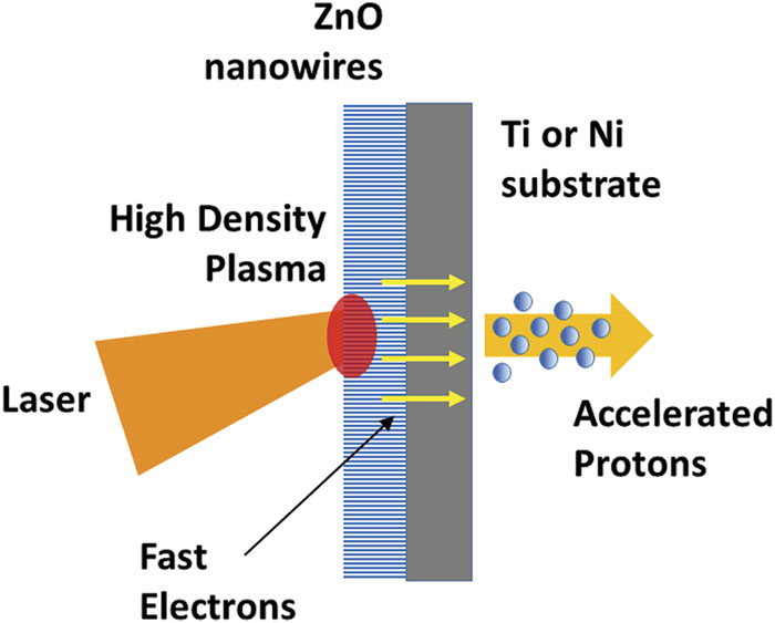
Here, we report in detail the methodologies used at the IMEM-CNR laboratories to fabricate targets that contain various types of ZnO nanowires grown over thin-foil substrates. These targets are then tested successively using the PW laser system available at the Intense Laser Irradiation Laboratory (ILIL).21 The decision to use a thin-foil substrate was dictated by the use of targets for proton acceleration via TNSA22 (Fig. 1). This application requires a relatively thin (micrometers thick) substrate.
![]()
Figure 1.Scheme showing proton acceleration via target normal sheath acceleration (TNSA) using nanowire-coated foils as targets.
The manufacturing process was optimized to provide accurate reproducibility of key parameters, the widest possible range, and a good homogeneity across the entire foil area (several cm2). The influence of various synthesis parameters on single–nanowire properties (length, diameter, alignment, density, etc.) is discussed to provide important guidelines for producing, when possible, micro or nanostructured thin-foil targets with desired characteristics.
II. EXPERIMENTAL METHODS
In order to provide a homogeneous distribution of ZnO nanowires and achieve similar results on thin foils made of different materials, a two-step synthesis process was required. The first step was designed to produce a continuous seed layer consisting of ZnO nanoparticles on one side of the thin foil, whereas the second step was intended to promote nanowire growth from this layer. Chemical solution methods were used for both steps.
The ZnO seed layer was obtained via the successive ionic layer adsorption and reaction (SILAR) method.23,24 This technique involves a series of rapid immersions in complementary reagent solutions (e.g., metal salt and alkaline solutions), which were alternated with rinsing in distilled water. It enables an almost layer-by-layer reaction to occur on the substrate surface. Equimolar zinc acetate and ammonia solutions (10 mM) were used to nucleate ZnO nanoparticles. A thin, continuous film was formed after 20–30 fast-cycle repetitions.
ZnO nanowires were then grown on this seed layer via chemical bath deposition. In order to obtain nanowires with various aspect ratios, alignments, and fill factors, various concentrations (10–200 mM) of hexamethylenetetramine (HMTA) and zinc acetate or zinc nitrate, with and without the addition of polyethylenimine (PEI), were investigated. The reactions occurred at 95 °C for between 1 and 6 h.
The procedure described above could be adapted to various substrate materials. Here, we used 5 and 12 μm-thick nickel (Ni) and titanium (Ti) foils. ZnO nanowires must be grown on only one side of the thin foil. The other side must be protected from oxidation, erosion, and other possible undesired reactions. Moreover, such thin foils are not easy to handle, especially in liquid processing environments. Thus, a holder was designed to hold a 1 × 1 in.2 square foil piece in position throughout all of the previously described operations (Fig. 2). The holder kept the foil stretched, protected its back side, and aided in placing it such that it faced towards the bottom of the reaction container at a 45° angle. This last precaution was intended to prevent other ZnO nanostructures that may grow in the solution volume from depositing on the foil surface via gravity, as this may interfere with nanowire growth.
![]()
Figure 2.(a) Exploded scheme showing the foil holder components. (b) Drawing of the assembled holder parts in the reaction solution.
The nanostructured foil was finally removed, rinsed with distilled water, and dried in vacuum. The entire foil piece was then suitable for placement in a multi-window target designed for multiple PW laser system tests.
III. RESULTS AND DISCUSSION
Top-down technologies such as photolithography, electrodeposition, and ion beam milling enable the production of accurate, regular patterns over various types of surfaces. Nevertheless, they can be quite time-consuming and expensive when applied to large areas. Moreover, these processes can be incompatible with some target materials or with the use of particularly thin foils, because of the reagents, solvents, or treatments used. For example, photoresist developers and removers, strong alkaline solutions used for alumina template dissolution, or the accumulation of surface electrostatic charge because of insufficient electrical conductivity can inhibit processes or be so aggressive that they oxidize or etch the target.
In contrast, bottom-up technologies are significantly cheaper and more scalable. Furthermore, they do not need templates or lithography masks. In these cases, dimensional control can be achieved via either thermodynamic or kinetic control and can easily be used to create arrays of nanostructures over vast areas (hundreds of cm2). However, these approaches do not provide the precise dimensional and positioning control associated with top-down methodologies. The patterns obtained are irregular on a micrometric scale but can be quite homogeneous across large areas and have reproducible size and density ranges once good control over the parameters that lead to nanostructure nucleation and growth is achieved.
ZnO nanowires have been grown at IMEM laboratories via both physical25,26 and chemical27,28 bottom-up methods. The former strategies can produce nanowires with higher purities and thus well-defined physical properties (e.g., electrical conductivity), but often involve high temperatures and oxidizing processes that are not suitable for thin metallic foils. In contrast, the chemical method described herein can be applied at lower temperatures (<100 °C) and in less aggressive environments. It can therefore be implemented using metallic substrates that are only a few micrometers thick. Most importantly, it is suitable for use with large-area substrates.
The process described herein is a two-step (i.e., seed-mediated growth) bottom-up process. The first step involved the deposition of a continuous ZnO nanoparticle seed layer onto the substrate of interest. In the second step, the seed layer acted as a nucleation center for subsequent ZnO nanowire growth. Control of the seed layer enabled growth of ZnO nanowires on various materials such as metal foils or wires, including low-wettability materials such as the graphitic surfaces of carbon fibers.27,28
The key parameter controlling the seed layer thickness was the deposition cycle, i.e. the number of sequential and alternating rinse and deposition steps in the SILAR procedure. Different materials typically require specific parameter tuning to obtain desired results. However, similar results were achieved by using Ni and Ti thin foils under similar conditions and 20–30 fast repetitions. Since no meaningful differences were found between the process steps, the substrate material and thickness are not considered in the following discussion regardless of which metal (Ni or Ti) or thickness (5 µm or 12 µm) was chosen for the foil target.
A substrate with insufficient or excessive seed layer deposition cycles can produce ZnO nanowire growth that is inhomogeneous with regard to either size or spatial distribution [Figs. 3(a)–3(c)]. In addition, providing metal foils with sub-micrometer surface roughness is equally important. Poor metal drawing may result in severe ZnO nanowire misalignment [Figs. 3(d) and 3(e)]. Good homogeneity can be achieved over large areas only when both these preliminary conditions are fulfilled and the deposition of other nanostructures from the solution is prevented [Figs. 3(f)–3(h)].
![]()
Figure 3.SEM images of inhomogeneous (x) and homogenous (✓) ZnO nanowire patterns: (a) and (b) inhomogeneity in size or alignment; (c) inhomogeneity in distribution across the thin foil; (d) and (e) inhomogeneity in height or orientation due to the irregular foil surface; (f), (g), and (h) large-scale homogeneity. Images (a), (c), (f), and (g) are taken with the foil parallel to the view, while images (b), (d), (e), and (h) are taken on tilted surfaces. Image (h) is taken on an intentionally broken film to show the ZnO nanowire patterned section.
Unfortunately, not all of the ZnO nanowire properties (length, diameter, density on the substrate, degree of alignment, and alignment direction) can be tuned independently during the second step of the bottom-up growth process.
A sketch of the main ZnO nanowire properties evaluated during this study is provided in Fig. 4. Some properties such as the length “l” and diameter “d” are related to the nanowires themselves. Others refer to the way that the nanowires grow compared to other nanowires or the foil surface. Examples include the angle “θ” formed with respect to the substrate normal and the nanowire-to-nanowire distance “δ.” The latter is clearly inversely proportional to the nanowire density. A fill-factor can also be defined as the planar ratio between the area occupied by nanowires and the total area (the sum of light gray hexagons vs the entire dark-gray rectangular area in the top right image of Fig. 4). This fill-factor is 100% for a continuous layer of merged nanowires but is for example ∼25% for a regular hexagonal close-packed pattern with δ = 2d. Since the nanowire pattern is generally irregular, we mainly discuss the average values of these quantities (as shown in the case of δ in the figure).
![]()
Figure 4.Graphic visualization of the main nanowire parameters: the nanowire length “l,” nanowire diameter “d,” nanowire-to-nanowire distance “δ,” and tilt angle “θ” with the line normal to the substrate.
During the growth, the ZnO nanowire length is determined mostly by the reaction time. Figure 5 shows various results obtained for nanowires with similar diameters and densities: the shortest nanowires [∼1 µm; Fig. 5(a)] are obtained after a 2 h reaction. The longest nanowires [∼5 µm; Fig. 5(c)] are obtained after 8 h. However, the nanowire length does not increase linearly with time. This is because the reagent concentration becomes depleted during the reaction and the growth rate decreases. Similarly, the reaction time needed to achieve a specific length may change if a substantially different reagent concentration is used.
![]()
Figure 5.SEM images of ZnO nanowires with similar diameters and different lengths. Each length is calculated via correction of image tilt.
The nanowire length is a crucial parameter that affects laser pulse absorption. Wires and structures with sizes or lengths on the order of tens or hundreds of nanometers tend to increase laser-target coupling with respect to a flat surface. This has been observed in experiments where rugged and coarse targets were used; this effect is produced mainly by multiple laser scattering on surface structures. However, the potential of nanostructures is fully exploited by using nanowires that are several micrometers long. In this case, their length matches the laser penetration depth and this condition results in the almost full absorption of laser light and in the volumetric heating of the target. As shown by Bargsten et al.8 via experiments and particle-in-cell simulations, a high-contrast relativistic laser pulse can penetrate into a high aspect-ratio nanowire array target for 4–5 µm before being absorbed completely. For targets intended for use in TNSA experiments, as in the present case, nanowires that are shorter than the optimal value do not maximize laser absorption. On the other hand, nanowires that are too long can result in a reduced coupling of hot electrons generated into the plasma with the substrate.
Nanowires up to 8 µm in length were produced. Larger solution volumes or a continuous reagent feed would be required to obtain even longer nanowires. However, such lengths are significantly higher than the estimated laser penetration distance;8 therefore, the ability to produce longer nanowires goes far beyond the goals of this study. Moreover, ZnO nanowires typically bend under their own weight when the length-to-diameter ratio is too high.26
Other key parameters that dictate laser–matter interactions are the thickness (diameter) of the nanowires in the array and the nanowire density (which determines the fill-factor parameter). Images of targets with various nanowire thickness and densities are reported in Fig. 6.
![]()
Figure 6.SEM images of nanostructured targets with different ZnO nanowire diameter and density ranges. Diameter ranges are labeled “THIN” for 50–150 nm, “MEDIUM” for 150–500 nm, and “HIGH” for 0.5 nm–1.5
The wire thickness can be controlled within certain tolerances from a thin 50–150 nm range (first row of the table in Fig. 6) to a thick 0.5–1.5 µm range (third row of the table in Fig. 6). The thickness is affected mainly by the use of shape-directing agents such as polyethylenimine (PEI). PEI is found to inhibit the development of ZnO nanowire sidewalls by adsorbing onto their nonpolar m-planes [presumably via the formation of PEI–Zn(II) ion complexes]. Moreover, it suppresses the homogeneous nucleation of zinc oxide clusters, thus promoting heterogeneous nucleation and growth.29
In contrast, the density is affected mainly by the reactant (zinc salt and HMTA) concentrations. The 20–100 mM range is proven to provide the best fill-factor results. Samples with low densities are shown in the first column of the table in Fig. 6, whereas samples with high spatial densities are shown in the third column.
Both the nanowire diameter and the array fill-factor parameters affect the laser light absorption efficiency as well as plasma evolution and homogenization at the end of the laser pulse. The roles of these parameters can be deduced by considering Fig. 7, which reports the change in the plasma kinetic energy normalized to the laser energy, i.e., the fraction of energy absorbed during irradiation of a silicon nanowire array target using a 25 fs laser pulse at an intensity of I = 5 × 10¹⁸ W/cm2. Results are presented for various combinations of nanowire diameters and fill factors by running fully kinetic particle-in-cell simulations using the code Aladyn in 2D Cartesian geometry.30 More details regarding these simulations can be found in reports by Sarkar et al.31 Even though the 2D geometry used in the simulation cannot quantify the absorption efficiency accurately, it can show the effects of various nanowire array parameters.
![]()
Figure 7.Energy absorbed by silicon nanowire array targets with various combinations of diameter d and gaps δ-d during irradiation with a 25 fs, 800 nm laser pulse at an intensity of 5 × 10¹⁸ W/cm2. The graphs are obtained by performing 2D, fully kinetic particle-in-cell simulations using the code Aladyn.
According to Fig. 7, if the gap (δ-d) between the wires is kept constant, absorption increases when the wire thickness d is reduced (compare the magenta, green, and red plots). This occurs because laser light can penetrate and therefore is absorbed only within ∼50–100 nm, which is on the order of the plasma skin depth. Nanowires with smaller diameters therefore contribute fully to laser absorption and are immediately ionized. The fast quivering of electrons out of the nanowire can lead to a Coulomb explosion and to a rapid homogenization of the plasma. When the nanowire size increases beyond the laser skin depth, i.e., exceeds 100 nm, the instantaneous absorption capabilities of the nanowire tend to saturate and the wire is progressively eroded by the laser pulse. The core of the wire remains at a temperature significantly lower than that of the plasma at its edge and is heated only by electron collisions and the return currents of cold electrons. When the diameter is several hundreds of nanometers, the wires remain present at the end of the laser interaction and the homogenization of the plasma requires more time.
The effect of density, i.e. of the distance between the nanowires, on laser absorption is determined mainly by the ability of laser light to propagate into the gaps. Laser light can propagate into gaps smaller than the diffraction limit by driving surface plasmon polaritons6,11 (SPPs) along the nanowire surface. The efficiency of SPP excitation increases with the gap size. This explains why the absorption efficiency rises in Fig. 7 when the gap is increased and the nanowire size is kept at comparable values.
In addition, it is worth considering that when the fill-factor increases, a larger portion of the laser pulse strikes the tips of the wires and is therefore back reflected without entering the array. Unfortunately, the fill-factor cannot be varied independently of the other parameters. It can only be tuned to a certain extent. For example, it is quite difficult to obtain a densely packed pattern of thin nanowires or a sparse distribution of thick microwires. This is because opposite and incompatible process parameters promote these aspects of nanowire growth. For instance, using PEI and a low reactant concentration (<20 mM) invariably leads to a sub-optimal areal homogeneity and a large variability in the nanorod aspect ratio. This can be explained by considering the coordinating effect of PEI with respect to Zn2+ moieties. Such interactions limit the availability of Zn sites at the lateral nanorod surfaces, thus preventing heterogeneous nucleation when the available amount of Zn2+ in solution is low. Similarly, using a Zn:HMTA ratio above 1:1 may lead to non-uniform growth of ZnO nanowires. When an excess of HMTA is present, the hydrolysis reaction favors the formation of the Zn[OH]42− intermediate, which is stable and soluble and depletes the Zn2+ cations that would otherwise be available for growth.
In addition, the nanowire alignment is strongly correlated with other nanowire properties. The denser and thicker the nanowires are, the more perpendicular is their alignment with respect to the surface (Fig. 8) and θ ≈ 0 is observed for most of the nanowires. Since this type of growth is not epitaxial on an oriented crystallographic surface, nanowire alignment seems to be affected more strongly by the presence of other nanowires growing nearby. Indeed, grown nanowires generally do not co-penetrate each other unless their thickness becomes comparable to or lower than the average nanowire-to-nanowire distance. Using a high ZnO:HMTA ratio (<2:1), without a co-surfactant or a shape-directing agent like PEI, significantly lowers the aspect ratio of the final ZnO nanowires. As a result, a film of aggregated parallelepiped hexagons is obtained [Fig. 8(c)].
![]()
Figure 8.SEM images of ZnO nanowires with various densities and alignments: (a) a low density and alignment with a broad θ range; (b) a high density and alignment with a narrow θ range centered around 0; and (c) a nearly continuous film of extremely high density microwires.
Optimization of the above growth parameters and a deeper understanding of the intrinsic limits of this technique enabled the production of targets for PW laser system tests. Micro and nanostructured targets were fabricated with different ZnO nanowire textures on several 1 × 1 square inch metal foil pieces. The foil pieces were suitable for fitting onto a holder designed with an array of windows to enable multiple PW laser system tests (Fig. 9).
![]()
Figure 9.SEM image of one of the windows in the target holder.
IV. CONCLUSIONS
The use of micro and nanostructured thin-foil targets in the context of high-intensity laser-target interactions was discussed and the roles of critical parameters in energy coupling and electron heating were highlighted. Targets suitable for ion acceleration experiments were produced by growing ZnO nanowires on the surface of 5 µm and 12 μm-thick foils made of nickel and titanium. The solution-based, two-step method enabled better control over random, self-assembly based, growth of the nanowires. The processing time, reagent concentration, and use of a seeding layer and polyethylenimine as shape-directing agents, enabled homogeneous growth of various nanowire patterns over areas several cm2 in size. Special attention was devoted to the control of the nanowire length, diameter, density, and alignment within specific ranges (i.e., lengths of 1–5 µm, diameters of 0.05–1.5 µm, and fill factors of 10%–50%) that play critical roles in attempts to optimize energy coupling in laser-target interaction experiments with a PW laser system.
ACKNOWLEDGMENTS
Acknowledgment. This research received funding from the Consiglio Nazionale delle Ricerche-funded Italian Research Network ELI-Italy (D.M. No. 631 08.08.2016). The authors thank P. Londrillo for fruitful and enlightening discussions on laser interactions with nanostructured targets.
References
[1] R.Loetzsch, O. N.Rosmej, L. P.Pugachev, S.Z?hter, C.Spielmann, D.Kartashov, M. E.Povarnitsyn, S.H?fer, M. C.Kaluza, N. E.Andreev, A.Schoenlein, Z.Samsonova, A.Hoffmann, I.Uschmann, C.Arda, D.Khaghani, A.Saevert. Generation of keV hot near-solid density plasma states at high contrast laser-matter interaction. Phys. Plasmas, 25, 083103(2018).
[2] Z. M.Sheng, D.Umstadter, K.Flippo, K.Mima, V. Y.Bychenkov, G.Mourou, A.Maksimchuk, Y.Sentoku. High-energy ion generation in interaction of short laser pulse with high-density plasma. Appl. Phys. B: Lasers Opt., 74, 207(2002).
[3] K.Gopal, D. N.Gupta, S.Kumar. Proton acceleration from overdense plasma target interacting with shaped laser pulses in the presence of preplasmas. Plasma Phys. Controlled Fusion, 61, 085001(2019).
[4] A.Giulietti, L. A.Gizzi, G.Cristoforetti, L.Fulgentini, F.Baffigi, S.Tudisco, P.Koester, A.Anzalone, G.D’Arrigo, L.Labate, G.Bussolino. Investigation on laser–plasma coupling in intense, ultrashort irradiation of a nanostructured silicon target. Plasma Phys. Controlled Fusion, 56, 095001(2014).
[5] G. S.Hicks, T.Ziegler, U.Schramm, H.Sakaki, Y.Watanabe, N.Iwata, H.Kiriyama, M. A.Alkhimova, N. P.Dover, A.Sagisaka, T. A.Pikuz, J. K.Koga, K.Zeil, E. J.Ditter, T.Miyahara, Y.Sentoku, Ko.Kondo, Z.Najmudin, M.Hata, M.Kando, M.Nishiuchi, A. Ya.Faenov, K.Kondo, A. S.Pirozhkov, O. C.Ettlinger, H. F.Lowe. Dynamics of laser-driven heavy-ion acceleration clarified by ion charge states. Phys. Rev. Res., 2, 033081(2020).
[6] F.Baffigi, G.Maero, L.Fulgentini, D.Terzani, G.Cristoforetti, A.Fazzi, L.Labate, M.Romé, D.Giove, R.Russo, P.Tomassini, F.Brandi, L. A.Gizzi, G.D’Arrigo, D.Palla, P.Koester. Laser-driven proton acceleration via excitation of surface plasmon polaritons into TiO2 nanotube array targets. Plasma Phys. Controlled Fusion, 62, 114001(2020).
[7] B. M.Luther, R.Hollinger, V. N.Shlyaptsev, C.Bargsten, A.Prieto, J. J.Rocca, A.Pukhov, S.Wang, L.Yin, M. A.Purvis, Y.Wang. Relativistic plasma nanophotonics for ultrahigh energy density physics. Nat. Photonics, 7, 796(2013).
[8] J.Park, M. G.Capeluto, R.Hollinger, S.Wang, A.Rockwood, M.Klapisch, V.Kaymak, A.Pukhov, J. J.Rocca, R.Tommasini, D.Keiss, C.Bargsten, R.London, V. N.Shlyaptsev, Y.Wang, M.Busquet. Energy penetration into arrays of aligned nanowires irradiated with relativistic intensities: Scaling to terabar pressures. Sci. Adv., 3, e1601558(2017).
[9] R.Hollinger, A.Townsend, J. J.Rocca, A.Pukhov, A.Prieto, V. N.Shlyaptsev, A.Curtis, C.Bargsten, A.Rockwood, Y.Wang, P.Stockton, M. G.Capeluto, V.Kaymak, S.Wang. Efficient picosecond x-ray pulse generation from plasmas in the radiation dominated regime. Optica, 4, 1344(2017).
[10] C.Riconda, A.Velyhan, M.Possolt, J.Pro?ka, J.Prok?pek, F.Réau, L.Labate, F.Baffigi, M.Passoni, A.Sgattoni, J.P?ikal, O.Tcherbakoff, L.Vassura, P.D’Oliveira, A.Bigongiari, F.Novotny, T.Ceccotti, M.Květon, V.Floquet, P.Martin, L. A.Gizzi, O.Klimo, A.Heron, M.Bougeard, L.?tolcoá, J.Fuchs, A.Macchi, M.Raynaud. Evidence of resonant surface-wave excitation in the relativistic regime through measurements of proton acceleration from grating targets. Phys. Rev. Lett., 111, 185001(2013).
[11] R.Russo, G.Maero, D.Palla, P.Koester, G.Cristoforetti, M.Romé, F.Baffigi, P.Tomassini, D.Giove, G.D’Arrigo, L. A.Gizzi, A.Fazzi, D.Terzani, L.Fulgentini, L.Labate, F.Brandi. Intense proton acceleration in ultrarelativistic interaction with nanochannels. Phys. Rev. Res., 2, 033451(2020).
[12] A.Macchi. Surface plasmons in superintense laser-solid interactions. Phys. Plasmas, 25, 031906(2018).
[13] Y.Gu, Y.Tang, W.Wu, Y.Ji, G.Jiang, C.Wang. Efficient generation and transportation of energetic electrons in a carbon nanotube array target. Appl. Phys. Lett., 96, 041504(2010).
[14] A.Handler, B. F.Shen, K. M.George, A.Zingale, D.Nasir, T.Rubin, J.Snyder, C.Willis, D. W.Schumacher, R. L.Daskalova, G. E.Cochran, P. L.Poole, L. L.Ji, E.Chowdhury. Relativistic laser driven electron accelerator using micro-channel plasma targets. Phys. Plasmas, 26, 033110(2019).
[15] Y.Wang, S.Kasdorf, S.Wang, A.Rockwood, A.Pukhov, C.Calvi, V. N.Shlyaptsev, R.Hollinger, J. J.Rocca, A.Moreau, A.Curtis, V.Kaymak, M. G.Capeluto. Enhanced electron acceleration in aligned nanowire arrays irradiated at highly relativistic intensities. Plasma Phys. Controlled Fusion, 62, 014013(2020).
[16] Z. G.Deng, S. C.Ruan, Z. Y.Chen, Y.Yin, H. B.Zhuo, T. P.Yu, D. Y.Yu, F. Q.Shao, M. Y.Yu, X. R.Jiang, D. B.Zou, C. T.Zhou. Enhancement of target normal sheath acceleration in laser multi-channel target interaction. Phys. Plasmas, 26, 123105(2019).
[17] F.Baffigi, G. R.Kumar, P. K.Singh, A. D.Lad, L. A.Gizzi, G.Chatterjee, D.Sarkar, M.Shaikh, R. G.Milazzo, G.D’Arrigo, P.Londrillo, J.Jha, G.Cristoforetti, M.Krishnamurthy, A.Adak. Transition from Coherent to Stochastic electron heating in ultrashort relativistic laser interaction with structured targets. Sci. Rep., 7, 1479(2017).
[18] H.Daido, A. S.Pirozhkov, M.Nishiuchi. Review of laser-driven ion sources and their applications. Rep. Prog. Phys., 75, 056401(2012).
[19] V. Yu.Bychenkov, V. T.Tikhonchuk, E.d’Humieres, A.Brantov. Optimization of laser-target interaction for proton acceleration. Phys. Plasmas, 20, 023103(2013).
[20] A.Sagisaka, Y.Watanabe, J. K.Koga, M. A.Alkhimova, A. S.Pirozhkov, Ko.Kondo, H.Sakaki, M.Nishiuchi, A. Ya.Faenov, K.Kondo, H.Kiriyama, Y.Sentoku, M.Hata, N. P.Dover, T.Miyahara, M.Kando, N.Iwata, T. A.Pikuz. Effect of small focus on electron heating and proton acceleration in ultrarelativistic laser-solid interactions. Phys. Rev. Lett., 124, 084802(2020).
[21] F.Brandi, L. A.Gizzi, P.Cirrone, G.Cristoforetti, D.Giove, C.Altana et al. A new line for laser-driven light ions acceleration and related TNSA studies. Appl. Sci., 7, 984(2017).
[22] M.Romé, L. A.Gizzi, P.Tomassini, L.Labate, G.Cristoforetti, D.Palla, F.Brandi, F.Baffigi, A.Fazzi, G.Bussolino, L.Fulgentini, P.Koester, G.Maero, D.Giove. Light ion accelerating line (L3IA): Test experiment at ILIL-PW. Nucl. Instrum. Methods Phys. Res., Sect. A, 909, 160(2018).
[23] Y. F.Nicolau. Solution deposition of thin solid compound films by a successive ionic-layer adsorption and reaction process. Appl. Surf. Sci., 22-23, 1061(1985).
[24] P. K.Nair, A. E.Jimenez-Gonzailez. Photosensitive ZnO thin films prepared by the chemical deposition method SILAR. Semicond. Sci. Technol., 10, 1277(1995).
[25] F.Pattini, D.Calestani, M.Villani, E.Gilioli, F.Bissoli, A.Zappettini. Solution-free and catalyst-free synthesis of ZnO-based nanostructured TCOs by PED and vapor phase growth techniques. Nanotechnology, 23, 194008(2012).
[26] L.Lazzarini, R.Mosca, M.Zha, M.Mazzera, L.Zanotti, A.Zappettini, D.Calestani. Large-area self-catalysed and selective growth of ZnO nanowires. Nanotechnology, 19, 325603(2008).
[27] M.Villani, M.Solzi, M.Culiolo, A.Zappettini, T.-Y.Kim, D.Calestani, D.Delmonte, S.-W.Kim, L.Marchini. Functionalization of carbon fiber tows with ZnO nanorods for stress sensor integration in smart composite materials. Nanotechnology, 29, 335501(2018).
[28] D.Delmonte, L.Marchini, M.Solzi, N.Coppedè, M.Villani, D.Calestani, A.Zappettini, R.Bercella, M.Culiolo. Turning carbon fiber into a stress-sensitive composite material. J. Mater. Chem. A, 4, 10486(2016).
[29] O.Chaix-Pluchery, V.Consonni, E.Appert, R.Parize, J. D.Garnier. Effects of polyethylenimine and its molecular weight on the chemical bath deposition of ZnO nanowires. ACS Omega, 3, 12457(2018).
[30] A.Sgattoni, P.Londrillo, G.Turchetti, C.Benedetti. ALaDyn: A high-accuracy PIC code for the Maxwell–Vlasov equations. IEEE Trans. Plasma Sci., 36, 1790(2008).
[31] P.Londrillo, A.Adak, A. D.Lad, M.Shaikh, P. K.Singh, D.Sarkar, M.Krishnamurthy, G.Ravindra Kumar, J.Jha, L. A.Gizzi, G.D’Arrigo, G.Cristoforetti, G.Chatterjee. Silicon nanowire based high brightness, pulse relativistic electron source. APL Photonics, 2, 066105(2017).

Set citation alerts for the article
Please enter your email address
© Copyright 2018-2021 | Chinese Laser Press. All Rights Reserved 沪ICP备15018463号-20