• Acta Photonica Sinica
  • Vol. 51, Issue 4, 0404002 (2022)
Guoping LUO*, Xingyuan CHEN, Sumei HU, and Weiling ZHU
Author Affiliations
  • School of Science,Guangdong University of Petrochemical Technology,Maoming,Guangdong 525000,China
  • show less
    DOI: 10.3788/gzxb20225104.0404002 Cite this Article
    Guoping LUO, Xingyuan CHEN, Sumei HU, Weiling ZHU. Near Infrared Hot Electrons Photodetectors Based on Tamm Plasmons[J]. Acta Photonica Sinica, 2022, 51(4): 0404002 Copy Citation Text show less

    Abstract

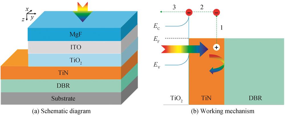
    Photodetection is an important means of modern detection and intelligent sensing technology. Classical photodetectors are based on the interband transition of electrons in the semiconductor materials, and their maximum response wavelength depends on the optical band gap of the semiconductor materials. Only photons with energy higher than the band gap (wavelength less than the maximum response wavelength) can be detected. Infrared photoelectric detectors are widely used in military reconnaissance, aerospace remote sensing, astronomical observation, industrial detection, optical fiber communication, infrared imaging and other fields. Common infrared detectors are made of semiconductor materials with extremely narrow band gap, which are facing many problems such as complex processes, high costs and low operation temperature. Hot electrons photodetectors based on the internal photoelectric effect have attracted tremendous attention in the past decade due to its advantages such as overcoming the response limitation of the semiconductor band gap, fast response speed, working at room temperature and light polarization sensitivity. The main problem of hot electrons photodetectors is low device responsivity, especially in the near infrared regions. In recent years, numerous studies at home and abroad have demonstrated that optical means such as grating plasmons, Tamm plasmons and micro-cavity effect can effectively enhance the optical absorption of metal films in the hot electrons photodetectors, and further improve the device responsivity. The planar metal thin films / Distributed Bragg Reflector (DBR) Tamm plasmons have many advantages such as simple structure, low manufacturing cost, high absorption efficiency. By changing the DBR structure parameters and metal thin films thickness, the resonance wavelength and maximum response wavelength can be adjusted. This structure provides an effective way to improve the absorption of hot electrons photodetectors, but the corresponding devices normally exhibits narrowband absorption and responsivity. The development of hot electrons photodetectors with broadband response characteristics is conducive to the expansion of its applications in optical fiber communication, photocatalysis, solar cells, solar water splitting and other fields. In view of broadband hot electrons photodetector, there are still some issues to be solved, such as narrow response spectra, low absorption efficiency, and low responsivity. TiN has high dielectric constants and excellent plasmons characteristics in the near infrared ranges. Moreover, the mean free path of hot electrons in the TiN thin films is about 50 nm, which is larger than the values of Au and Ag. Therefore, TiN is considered as potential candidate which can be used to achieve high performance broadband hot electrons photodetectors. In this study, we propose a multi-layer device architecture based on the TiN/TiO2 Schottky barrier and the Tamm plasmons formed by the TiN/ DBR structure to achieve high-performance broadband near infrared hot electrons photodetectors. This architecture has the following characteristics: 1) The TiN/DBR Tamm plasmons with manipulating the DBR structural parameters are able to enhance broadband absorption of the TiN thin films and broaden the device response spectra; 2) The Schottky barrier of TiN/TiO2 is only 0.37 eV, which will be beneficial to the transporting of low energy hot electrons; 3) The MgF anti-reflectance layer is used to reduce optical loss. Based on the optical transfer matrix and hot electrons emission theory, we firstly simulated the reflection and absorption spectra of the hot electrons photodetectors. Furthermore, we calculated the corresponding device responsivity. The simulation results show that with high refractive indices ratio dielectric layers, the DBR form by Ge/SiO2 can effectively expand the absorption spectra of the TiN thin films and the device response spectra. The absorption of TiN thin films and device responsivity also can be largely enhanced. By adjusting the DBR structural parameters, such as dielectric layers, DBR period and the DBR center wavelength, the absorption spectra of TiN thin films and the responsivity spectra of the hot electrons devices can be regulated. We also discuss the influences of the thickness of TiN thin films and MgF anti-reflectance layer. The maximum absorption of the TiN thin films is 99.8%, and the maximum responsivity value of the optimized device is 29.2 mA/W. The full width at half maximum of the response spectra is about 900 nm. The simulation results indicate that as the incident angle increases from 0 to 30°, the Tamm state can still be excited, but the peak absorption of the TiN thin films and the device responsivity are decreased. The peak absorption and response wavelength under the TE polarization and TM polarization are both blue shifted with the increasing of incident angles. This multi-layer device architecture provides a new route to realize high-performance broadband near infrared hot electrons devices. Meanwhile, it is beneficial to expand the applications of hot electrons photodetectors.
    Guoping LUO, Xingyuan CHEN, Sumei HU, Weiling ZHU. Near Infrared Hot Electrons Photodetectors Based on Tamm Plasmons[J]. Acta Photonica Sinica, 2022, 51(4): 0404002
    Download Citation