
Jun Wang, Meiyu He, Xingwei Han, Chao Han, Jiayue Han. Localized field enhanced graphene-based near-infrared photodetector (Invited)[J]. Infrared and Laser Engineering, 2022, 51(1): 20210823
- Infrared and Laser Engineering
- Vol. 51, Issue 1, 20210823 (2022)
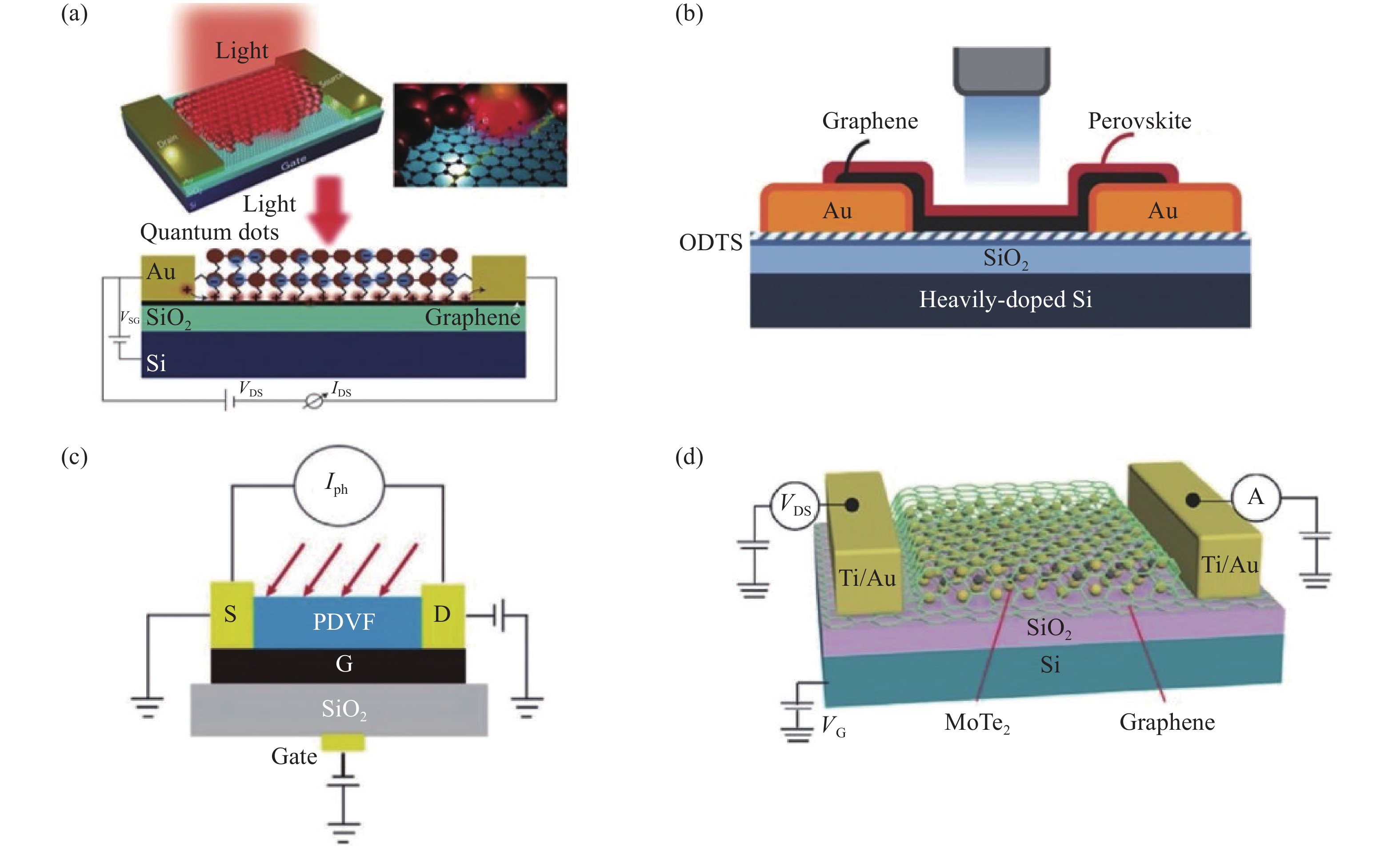
Fig. 1. Typical structure of single absorption layer graphene detector based on localized filed enhancement. (a) Structural diagram of the graphene/PbS phototransistor; (b) Structural diagram of the graphene/perovskite phototransistor; (c) Structural diagram of the graphene/PDVF phototransistor; (d) Structural diagram of the graphene/MoTe2 phototransistor
![Typical structure of graphene detector based on plasmon resonance filed enhancement. (a) Structural diagram of the graphene/gold nanoparticle photodetector[13]; (b) Structural diagram of the graphene/Si QDs phototransistor[14]](/richHtml/irla/2022/51/1/20210823/img_2.jpg)
Fig. 2. Typical structure of graphene detector based on plasmon resonance filed enhancement. (a) Structural diagram of the graphene/gold nanoparticle photodetector[13]; (b) Structural diagram of the graphene/Si QDs phototransistor[14]
Fig. 3. Typical structures of graphene detectors enhanced by localized field with double absorption layers. (a) Structural diagram of the graphene/PTCDA/pentacene phototransistor[15]; (b) Structural diagram of the graphene/PTAA/perovskite phototransistor[16]; (c) Structural diagram of the graphene/C 60/pentacene phototransistor[17]; (d) Response characteristics with different wavelengths[18]
Fig. 4. Injection layer structure NIR graphene/organic phototransistor. (a) Structural diagram; (b) Pulse signals in calm state and after exercise[21]
Fig. 5. Graphene heterojunction device with all-optically modulated photonic synapses function. (a) Device heterostructure diagram of the photonic synapse;(b) EPSC and IPSC of the device triggered by an optical pulse with wavelengths of 980 and 450 nm, respectively[22]
Fig. 6. Visible and near infrared bidirectional light modulation. (a) Variation of photocurrent of visible Light under Near-infrared Modulation (5 nm C 60 device)[23]; (b) Variation of photocurrent of visible Light under Near-infrared Modulation (11.2 nm C 60 device)[23]; (c) Change of response speed of Near-infrared Light under visible light modulation (11.2 nm C 60 device)[23]

Set citation alerts for the article
Please enter your email address
© Copyright 2018-2021 | Chinese Laser Press. All Rights Reserved 沪ICP备15018463号-20