
Changjiang ZHAO, Chao MA, Juncheng LIU, Zhigang LIU, Yan CHEN. Sputtering Power on the Microstructure and Properties of MgF2 Thin Films Prepared with Magnetron Sputtering [J]. Journal of Inorganic Materials, 2020, 35(9): 1064
- Journal of Inorganic Materials
- Vol. 35, Issue 9, 1064 (2020)
Abstract
Solar cell is one of the main power sources of various space equipment, such as satellite, space workstation, planet lander, etc. The service environment of space solar cell is rather harsh, where the temperature fluctuates greatly, and there are also many cosmic ray radiations and high-energy particle impacts[
One of the reasons for the loss of solar cell conversion efficiency is that the photovoltaic glass or the cover glass has a reflection loss of nearly 10% to the incident sunlight. The most direct and convenient way to increase the conversion efficiency of the solar cells is to reduce the surface reflectivity of the cells and increase the absorption of sunlight. One of the most commonly used methods of antireflection is to coat a layer of antireflection film on the surface of the glass cover, that is, to coat one or more layers of optical film on the surface of the optical element, to reduce the light reflection and increase the light transmittance through the interference of light[
MgF2 film is one of the most widely used antireflection films because of its wide transmission spectrum, good chemical stability, radiation resistance and mechanical properties[
The principle of magnetron sputtering is to bombard the target with high energy ions. The target materials are sputtered to the substrate surface in the form of ions, atoms or molecules to form thin films. Its advantages are obvious, include the high density of film, the strong adhesion between the film and the substrate, and the high preparation efficiency. However, its disadvantages are also apparent. The main one is that in the sputtering of fluoride, oxides and other compounds, most of the target materials are not sputtered out and deposited on the substrate surface in molecular form, and the film has some chemical composition deviation. The main defect of MgF2 thin film prepared by magnetron sputtering is the F deficiency. The atom ratio of F to Mg is difficult to reach the ideal stoichiometric ratio of 2 : 1. There are a few of factors that affect the extent of F deficiency, including the quality of target material, the composition and ratio of sputtering gas, the sputtering processing parameters, such as the gas pressure, the substrate temperature, the sputtering power and so on. When the target and working gas are determined, the sputtering power has an important influence on the F: Mg atomic ratio of the film. Kawamata, et al. [
In this work, SF6 was added to the working gas Ar2 as the reactive gas, and MgF2 thin films were deposited on quartz glass substrates via RF magnetron sputtering with high pure MgF2 target. The effects of sputtering power on the structure and optical properties of MgF2 thin films were investigated.
1. Experimental
1.1 Film preparation
The light transmission process in the system of Air/MgF2 thin film (refractive index 1.38)/quartz glass substrate (refractive index 1.46, thickness 1.0 mm) was simulated with G-solver software. The optimal thickness of MgF2 thin film was determined to be 70 nm, and the highest integral transmittance within 300-1100 nm, i.e., the film transmittance, to be 94.51%.
MgF2 thin films were deposited on quartz glass (99.9%, 50 mm×25 mm×1 mm) via RF magnetron sputtering with MgF2 target (Ф101.6 mm×3 mm, 99.99%, Nanchang Guocai Technology Co., Ltd., China). Before sputtering, the quartz glass pieces were cleaned with ultrasonic 15 min with decontamination powder, acetone, anhydrous ethanol and deionized water in turn, and then dried in a drying oven for standby; the working gas was high-purity Ar2 (99.999%), SF6 (99.999%) with a flow ratio of 5% was added as the reactive gas, and the background vacuum degree was 6.0×10⁻⁴ Pa; the sputtering working pressure was 2.0 Pa; the RF power supply was set to 115, 150, 185, and 220 W, respectively; the target was pre-sputtered for 10 min before deposition to clean the target surface, stabilize the working pressure and RF power.
1.2 Characterization
X-ray photoelectron spectroscopy (XPS, K-alpha, Thermo-fisher, USA) was used to qualitatively and quantitatively analyze the chemical composition of the film. X-ray diffraction (XRD, D8 Discover, Bruker, Germany) was used to analyze the crystal structure of the film, and the measuring angle ranged from 10° to 80°. The surface morphology of the film was observed with field emission scanning electron microscope (FE-SEM, S4800, Hitachi, Japan). The thickness and refractive index of the film were determined with a spectrum ellipsometer (COSE- DVN-D-C, Syscos Instrument Technology (Shanghai) Co., Ltd, China). The film’s transmittance spectrum within 300-1100 nm was reordered with an ultraviolet- visible near infrared spectrophotometer (UV-Vis-NIR, UH4150, Hitachi, Japan).
2. Results and discussion
2.1 F: Mg molar ratio of thin films
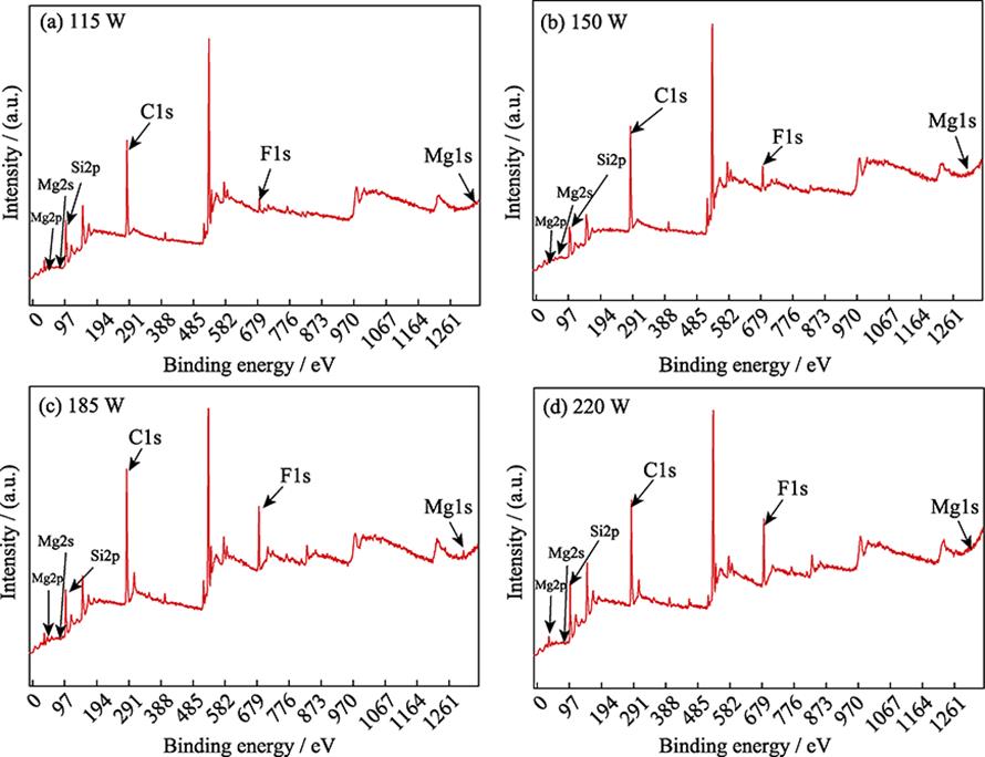
The XPS spectra of MgF2 films are shown in Fig. 1. From Fig. 1 (a-d), the film mainly contains F, Mg, C, Si elements. Among them, C may be from the CO2 adsorbed from the atmosphere during the sample storage and transfer process or the adhered organic matter from the transparent plastic sample bag; Si should come from the glass substrate. It can be found that the height of F1s peak in Fig. 2(b) is significantly higher than that in Fig. 2(a); the height of F1s peak in Fig. 2(c) or (d) is much higher than that in Fig. 2(b). This means that the relative content of F in the film increases with the sputtering power.
![]()
Figure 1.Effect of sputtering power on XPS spectrum of MgF2 film
The molar ratios of F to Mg in the films prepared at different sputtering powers were determined to be 1.65 (115 W), 1.88 (150 W), 2.02 (185 W), and 2.44 (220 W), respectively, with calculation according to the intensities of Mg and F peaks in each figure and an appropriate sensitivity factor. It can be seen that with the increase of sputtering power, the molar ratio of F: Mg increases continuously, and 2.02 at 185 W is the closest to the ideal stoichiometric ratio of 2 : 1. This is mainly because with the increase of sputtering power, the ionized F- ratio from SF6 increases gradually, so the molar ratio of F to Mg in the film also increases.
Tuszewski, et al. [
2.2 Micro structure
Fig. 2 shows the XRD patterns of the prepared MgF2 films.
![]()
Figure 2.Effect of sputtering power on XRD pattern of MgF2 thin film
It can be seen from the figure that, in the first three diffraction patterns of the thin films with power of 115, 150, and 185 W, only the characteristic diffraction peak of (220) crystal plane appears near 2θ=56°, the main characteristic diffraction peak of (110) crystal plane and other characteristic diffraction peaks of (111) crystal plane and (211) crystal plane do not appear; while in the diffraction pattern of the thin film with power of 220 W, there is no diffraction peak. Secondly, when the power increased from 115 W to 185 W, the characteristic diffraction peak of (220) crystal plane firstly became sharper then widened, and its intensity firstly increased greatly then decreased rapidly; when the power reached 220 W, this diffraction peak disappeared. It indicates that with the increase of sputtering power, the diffraction peak intensity firstly increases and then decreases, while the half peak width firstly decreases and then increases.
The intensity, position angle and FWHM (Full width at half maximum) of the diffraction peak of (220) crystal plane of each film, as well as the molar ratio of F to Mg, are listed in Table 1.
| Sample | 2 | Intensity/(a.u.) | FWHM | Interplanar spacing/nm | Grain size/nm | |
|---|---|---|---|---|---|---|
| 115 W | 1.65 | 57.832 | 127 | 0.95 | 0.1593 | 9.6 |
| 150 W | 1.88 | 56.447 | 36086 | 0.534 | 0.1629 | 17.2 |
| 185 W | 2.02 | 56.968 | 158 | 0.874 | 0.1615 | 10.4 |
| 220 W | 2.44 | Amorphous | - | - | - | - |
Table 1.
Molar ratio of F to Mg and XRD analysis results of MgF2 films
According to the Scherrer formula D = Kλ/βcosθ (where D is the grain size, K is the Scherrer constant, conventionally set at 0.89, λ is the X-ray wavelength 0.154056 nm, β is the corrected FWHM of (222) plane diffraction peak, and θ is Bragg’s diffraction angle), the calculated average grain sizes of these three samples are 9.6, 17.2 and 10.4 nm, respectively, which are also listed in Table 1. In addition, the lattice constants of the crystal were refined with Jade analysis software, which are also listed in Table 1. With the sputtering power increase from 115 W to 150 W, the interplanar spacing of (220) crystal plane of the film increases from 0.1593 nm to 0.1628 nm, and then decreases to 0.1615 nm at 185 W. The grain size also changes with the increase of sputtering power. When the sputtering power increases from 115 W to 150 W, the grain size increases from 9.6 nm to 17.2 nm. As the power further increases to 185 W, the grain size decreases to 10.4 nm. Both the FWHM change of the diffraction peak of (220) crystal plane and the that of the grain size confirm the change of the crystalline state of the film with the sputtering power.
The absence of characteristic diffraction peaks of (110), (111) and (211) crystal planes may be due to the preferred orientation of the sputtered particles during deposition and crystallization. Compared with (110), (111), (211) crystal planes, the interspacing between (220) crystal planes is smaller (PDF 41-413), and the <220> crystal orientation is in the direction of non-dense arrangement of atoms, so it is easier for particles to adhere along the <220> crystal orientation. When the sputtering power was low, the crystallinity of the film was also low. Firstly, the molar ratio of F to Mg was only 1.65 : 1, far away from the ideal chemical ratio of 2 : 1, as described in Section 2.1. Secondly, the energy of the sputtered particles was low, which was not conducive to the combination and crystallization of particles. When the sputtering power increased, the molar ratio of F to Mg was closer to the ideal chemical ratio of 2 : 1, and the sputtered particles also obtained higher energy, which was conducive to the combination and crystallization of particles. When the sputtering power was too high, firstly, the molar ratio of F to Mg was again far away from the ideal chemical ratio; secondly, the output of the sputtered particles, the energy of the particles and the deposition rate of the film were greatly increased, and the combination and reaction time between the particles were shortened; thirdly, the high-energy particles might impact the deposited particles, resulting in the secondary sputtering. All of these were not conducive to the combination and crystallization of particles, so the crystallinity of the film seriously decreased, and finally became amorphous.
2.3 Surface morphology
The surface micro morphologies of MgF2 films are shown in Fig. 3. It can be seen that the sputtering power has a significant effect on the surface morphology of MgF2 film. First, all film surfaces are very compact. Comparing Fig. 3(a) with Fig. 3(b), we can see that after the sputtering power increased from 115 to 150 W, the profile of particles on the film surface became clearer, and particle size increased slightly. When the sputtering power increased from 150 W to 185 W, the particle size continued to increase, forming a white network between the particles, as shown in Fig. 3(c). When the sputtering power continued to increase to 220 W, the profile of the particles on the film surface became blurred, as shown in Fig. 3(d). The change of the film surface micro morphology corresponds to that of the film crystallinity. However, we can see that the particle size shown in Fig. 3 is much larger than the grain size in Table 1, it’s due to the fact that a single particle should be composed of many grains that aggregated together.
![]()
Figure 3.Effect of sputtering power on the surface micro morphology of MgF2 film
2.4 Optical properties
Fig. 4 shows the refractive index spectra of MgF2 films. It can be seen from Fig. 4 that, as the incident wavelength increases from 300 nm to 1100 nm, the refractive index of the film decreases gradually. Secondly, with the increase of sputtering power, the refractive index of the film decreases first and then increases; when the sputtering power is 185 W, the refractive index of the film is the lowest. Table 2 lists the thicknesses of the films, the refractive indexes within 300-1100 nm and the refractive indexes at 550 nm of the films prepared at different sputtering powers. It can be seen that with the increase of sputtering power, the refractive index at 550 nm decreases from 1.501 to 1.384, which is very close to that of the MgF2 bulk crystal, 1.38, and then increases to 1.484.
![]()
Figure 4.Effect of sputtering power on refractive index spectra of MgF2 thin film
| Sputtering power/ | Thickness/ | Refractive index within | Refractive index at | Integral transmittance |
|---|---|---|---|---|
| 115 | 65 | 1.525-1.494 | 1.501 | 92.489 |
| 150 | 63 | 1.483-1.452 | 1.459 | 93.433 |
| 185 | 67 | 1.408-1.377 | 1.384 | 94.990 |
| 220 | 76 | 1.508-1.477 | 1.484 | 92.925 |
| Glass | 0 | 1.46 | 93.20 |
Table 2.
Thickness, refractive index and integral transmittance of MgF2 film
The change of refractive index is mainly due to the fact that molar ratio of F: Mg. MgF2 is the lowest refractive index substance in nature. Once the molar ratio of F to Mg deviates from the ideal chemical ratio 2 : 1, the refractive index of MgF2 will become larger. Secondly, it comes from the change of crystallinity state. When the crystallinity of the film increases, the defects in the film reduces, so does the interference to the optical transmission, thus the refractive index decreases. But the effect of the latter is far less than that of the former. Therefore, when the sputtering power is 185 W, the ratio of F to Mg in the film is 2.02, closest to the idea stoichiometric ratio of 2 : 1, the refractive index is the lowest.
Fig. 5 shows the transmittance spectra of the glass cover coated MgF2 films (hereinafter referred to as the film transmittance spectrum) and that of the bare glass substrate within 300-1100 nm. It can be seen from the figure that, firstly, both the film transmittance and the glass substrate transmittance increase with the increase of wavelength. Secondly, all the film spectra intersect with the substrate spectrum. The wavelength of the junction firstly decreases and then increases with the increase of sputtering power. The junction wavelengths are about 930, 580, 430 and 500 nm, respectively. That is to say, the junction first moves to the left and then to the right. At the right of the junction, the transmittance of film is higher than that of the substrate; at the left of the junction, the transmittance of film is lower than that of the substrate. According to the visual inspection, the integrated transmittance of 115 W film should be lower than that of the glass substrate, and the transmittance of other films may be higher than that of the substrate. Moreover, the cross point of 185 W film spectrum with that of the substrate is on the left of other cross points, and the transmittance of 185 W film on the right is far higher than that of other films, so the integrated transmittance of 185 W film should be the highest.
![]()
Figure 5.Effect of sputtering power on transmission spectra of MgF2 thin film
To integrate all transmittance spectra, the specific transmittance values are also listed in Table 2. It can be seen that with the increase of sputtering power from 115 W to 220 W, the transmittance of the thin film first increases from 92.498% to 94.99%, and then decreases to 92.925%; only the transmittance of the thin film prepared at 150 or 185 W power is higher than that of the glass substrate, 93.2%, realizing the antireflection function. Fig. 6 is based on the data in Table 2, shows more intuitively that the transmittance (300-1100 nm) of the film has a good corresponding relationship with the refractive index at 550 nm, that is, the transmittance increases with the decrease of the refractive index, and decreases with the increase of the refractive index. As stated in the experimental section, the optimal thickness of MgF2 film is 70 nm, and the integral highest transmittance calculated with G-solver software is 94.51%. The experimental results show that the transmittance of film prepared at 185 W is 94.99%, which is about 0.5% higher than the calculated value, and about 1.79% higher than that of the bare glass substrate.
![]()
Figure 6.Relation between integrated transmittance within 300-1100 nm and refractive index of thin film at 550 nm
3. Conclusions
F deficiency is a common defect of MgF2 thin films prepared with sputtering and evaporation. In order to reduce the F deficient defect in MgF2 thin films prepared by magnetron sputtering, SF6 was added to the working gas Ar2 as the reactive gas, MgF2 thin films were prepared on quartz glass substrates with RF magnetron sputtering. The chemical composition of the film was quantitatively analyzed with XPS, the microstructure of the film was analyzed with XRD, and the surface micromorphology of the films was observed with SEM, the transmittances of MgF2 film and glass substrate were measured with UV-Vis-NIR spectrometer, and the thickness and refractive index of the film were measured by spectrum ellipsometer. The effects of sputtering power on the structure and properties of MgF2 films were investigated. The main conclusions are as follows:
1) With the sputtering power increase from 115 to 220 W, the atomic ratio of F to Mg increases continuously; at 185 W, the atomic ratio of F to Mg reaches 2.02, closest to the ideal stoichiometric ratio of 2 : 1.
2) The crystallinity of MgF2 film increases first, then decreases, and finally changes into amorphous state with the increase of sputtering power; when the power is 150 W, the crystallinity is the highest. The particle profile of MgF2 film surface becomes clearer at first, and the particle size increases slightly, finally the particle profile becomes blurred.
3) The refractive index of MgF2 film decreases firstly and then increases with the increase of sputtering power. When the power is 185 W, the lowest refractive index at 550 nm of MgF2 film is 1.384, close to that of MgF2 bulk crystal.
4) The integral transmittance of the coated glass at 300-1100 nm reaches 94.99% when the sputtering power is 185 W, which increases the transmittance of the glass substrate by 1.79%.
References
[1] Y WANG, R CUI, X XU. Recent progress and prospect of space solar cells. Chin. J. Power Sources, 25, 1182-1185(2001).
[2] Z LIU, F WANG, Y CHEN. Impact analysis and solution of solar array design in Martian surface environment. Spacecraft Engineering, 25, 39-45(2016).
[3] X LUO. Design and Preparation of TiO2-based Anti-reflection Films. Changsha: Hunan University Doctoral dissertation(2011).
[5] A ALEMU, A FREUNDLICH, N BADI. Low temperature deposited boron nitride thin films for a robust anti-reflection coating of solar cells. Sol Energ. Mat. Sol C, 94, 921-923(2010).
[6] M CID, N STEM, C BRUNTTI. Improvements in antireflection coatings for high efficiency silicon solar cells. Surf. Coat. Tech., 106, 117-120(1998).
[8] K HANNES, E KEMNITZ, A HERTWIG. Transparent MgF2 films by Sol-Gel coating: synthesis and optical properties. Thin Solid Films, 516, 4175-4177(2008).
[9] J NOACK, K SCHEURELL, E KEMNITZ. MgF2 antireflective coatings by Sol-Gel processing: film preparation and thermal densification. J. Mater. Chem., 22, 18535-18541(2012).
[10] E LEE S, W CHOI S, J YI. Double-layer anti-reflection coating using MgF2 and CeO2 films on a crystalline silicon substrate. Thin Solid Films, 376, 208-213(2000).
[11] S MERTIN, L MRAOT, S SANDU C. Nanocrystalline low refractive magnesium fluoride films deposited by reactive magnetron sputtering: optical and structural properties. Adv. Eng. Mater., 17, 1652-1659(2015).
[12] K KAWAMATA, T SHOUZU, N MITAMURA. K-M-S (keep-molecules sputtering) deposition of optical MgF2 thin films. Vacuum, 51, 559-564(1998).
[13] M TUSZEWSKI, K SCARBOROUGH W, R WHITE R. Spectrometry of 0.46 and 13.56 MHz Ar/SF6 inductive plasma discharges. J. Appl. Phys, 96, 1811-1818(2004).


Set citation alerts for the article
Please enter your email address

© Copyright 2018-2021 | Chinese Laser Press. All Rights Reserved 沪ICP备15018463号-20