• Photonics Research
  • Vol. 10, Issue 12, 2876 (2022)
Xufeng Jing1、2、*, Guihong Qin1、2, and Peng Zhang1
Author Affiliations
  • 1Institute of Optoelectronic Technology, China Jiliang University, Hangzhou 310018, China
  • 2Centre for THz Research, China Jiliang University, Hangzhou 310018, China
  • show less
    DOI: 10.1364/PRJ.476100 Cite this Article Set citation alerts
    Xufeng Jing, Guihong Qin, Peng Zhang. Broadband silicon-based tunable metamaterial microfluidic sensor[J]. Photonics Research, 2022, 10(12): 2876 Copy Citation Text show less
    (a) and (b) are schematics of arrays and element structures, respectively. (c) Absorption rate, reflectivity, and transmittance of metamaterial absorbers.
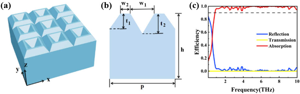
    Fig. 1. (a) and (b) are schematics of arrays and element structures, respectively. (c) Absorption rate, reflectivity, and transmittance of metamaterial absorbers.
    (a) Absorption of terahertz waves by the substrate; (b) absorption of terahertz waves by the quadrangle structure; (c) absorption of terahertz waves by inverted pyramid structures; (d) absorption of terahertz waves by the combination of a quadrangle in a pyramidal structure.
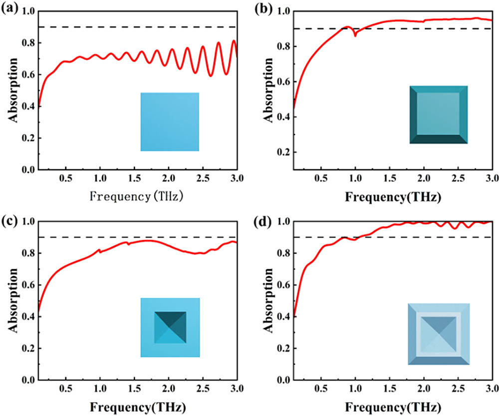
    Fig. 2. (a) Absorption of terahertz waves by the substrate; (b) absorption of terahertz waves by the quadrangle structure; (c) absorption of terahertz waves by inverted pyramid structures; (d) absorption of terahertz waves by the combination of a quadrangle in a pyramidal structure.
    (a), (c), (e) Distribution of electric fields and time-averaged power flow (red arrows) in the xoz plane; (b), (d), (f) magnetic field distribution and time-averaged power flow diagram in the yoz plane (red arrow); (g) is a diffraction efficiency (DE) plot in the range of 0.1–3 THz.
    Fig. 3. (a), (c), (e) Distribution of electric fields and time-averaged power flow (red arrows) in the xoz plane; (b), (d), (f) magnetic field distribution and time-averaged power flow diagram in the yoz plane (red arrow); (g) is a diffraction efficiency (DE) plot in the range of 0.1–3 THz.
    (a) and (b) are absorption spectra of different incident angles in TE and TM modes, respectively.
    Fig. 4. (a) and (b) are absorption spectra of different incident angles in TE and TM modes, respectively.
    Absorption spectra of different structural parameters.
    Fig. 5. Absorption spectra of different structural parameters.
    (a) and (b) show the relationship between the doped silicon carrier concentration and the plasma frequency and the depth z under different pump lights, respectively.
    Fig. 6. (a) and (b) show the relationship between the doped silicon carrier concentration and the plasma frequency and the depth z under different pump lights, respectively.
    Calculated carrier concentration (curve) approximated to the carrier concentration in the hierarchical model (histogram).
    Fig. 7. Calculated carrier concentration (curve) approximated to the carrier concentration in the hierarchical model (histogram).
    (a) Absorption spectra under pump light regulation of different energy densities; (b) modulation depth at two frequency points of 0.8 and 1.1 THz.
    Fig. 8. (a) Absorption spectra under pump light regulation of different energy densities; (b) modulation depth at two frequency points of 0.8 and 1.1 THz.
    Flow chart of the production of the absorber.
    Fig. 9. Flow chart of the production of the absorber.
    (a) Single-bar compensation structure; (b) L-type compensation structure; (c) T-type compensation structure; (d) compensatory structural element structures; (e) compensatory structural periodic structures.
    Fig. 10. (a) Single-bar compensation structure; (b) L-type compensation structure; (c) T-type compensation structure; (d) compensatory structural element structures; (e) compensatory structural periodic structures.
    (a) KOH + IPA corrosion for 30 min; (b) TMAH + IPA corrosion for 60 min; (c) TMAH + Triton x-100 corrosion for 60 min.
    Fig. 11. (a) KOH + IPA corrosion for 30 min; (b) TMAH + IPA corrosion for 60 min; (c) TMAH + Triton x-100 corrosion for 60 min.
    (a) Physical view of a metamaterial absorber; (b) step meter measured depth map; (c) simulation and experimental testing of absorption rates.
    Fig. 12. (a) Physical view of a metamaterial absorber; (b) step meter measured depth map; (c) simulation and experimental testing of absorption rates.
    (a) Schematic diagram of the material to be measured coated on the surface of the metamaterial; (b) refractive index detection characteristics of the sensor; (b) refractive index detection characteristics of the sensor under different thicknesses of the substance to be measured.
    Fig. 13. (a) Schematic diagram of the material to be measured coated on the surface of the metamaterial; (b) refractive index detection characteristics of the sensor; (b) refractive index detection characteristics of the sensor under different thicknesses of the substance to be measured.
    (a) Integrated microflow channel sensor based on a metamaterial absorber; (b) relationship between the absorption peak of the microflow channel sensor and the refractive index.
    Fig. 14. (a) Integrated microflow channel sensor based on a metamaterial absorber; (b) relationship between the absorption peak of the microflow channel sensor and the refractive index.
    (a) At different channel thicknesses h1, the relationship between the absorption peak and the refractive index n of the analyte; (b) relationship between the absorption peak and the refractive index n of the analyte at different top cover thicknesses h2; (c) relationship between the absorption peak and the refractive index n of the analyte under different cap refractive indices ncap.
    Fig. 15. (a) At different channel thicknesses h1, the relationship between the absorption peak and the refractive index n of the analyte; (b) relationship between the absorption peak and the refractive index n of the analyte at different top cover thicknesses h2; (c) relationship between the absorption peak and the refractive index n of the analyte under different cap refractive indices ncap.
    (a) Microflow channel sensor preparation flow chart; (b) physical drawing of the microflow channel sensor.
    Fig. 16. (a) Microflow channel sensor preparation flow chart; (b) physical drawing of the microflow channel sensor.
    (a), (b), and (c) are the simulated (black) and test (red) reflectance plots for air, alcohol, and water, respectively; (d), (e), and (f) are the simulated (black) and test (red) absorbance plots for air, alcohol, and water, respectively.
    Fig. 17. (a), (b), and (c) are the simulated (black) and test (red) reflectance plots for air, alcohol, and water, respectively; (d), (e), and (f) are the simulated (black) and test (red) absorbance plots for air, alcohol, and water, respectively.
    ReferencesStructureMaterialAbsorption Band (A>90%)SwitchableEtching Process
    [77]Square silicon ringSilicon0.5–5.7 THzNoNo experimental validation
    [69]H-shapedSilicon0.59–1.49 THzYesDry etching
    [78]Rings and cylindrical disksSilicon0.95–2 THzYesDry etching
    [44]Double-layer binary gratingsSilicon, SU-80.44–10 THzNoDry etching
    [79]Binary gratingSilicon, SU-80.3–3 THzNoNo experimental validation
    This workSquare silicon ringSilicon0.8–10 THzYesWet etching
    Table 1. Comparison Table of Different Types of All-Media Absorbers
    Refractive IndexFWHM (THz)S (GHz/RIU)QFOM
    1.00.02141.843
    1.20.03156724.52918.173
    1.40.03944117.36211.307
    1.60.04733713.0827.232
    1.80.05227010.5835.143
    Table 2. Performance Parameters of Microfluidic Sensors at Different Refractive Indices
    Xufeng Jing, Guihong Qin, Peng Zhang. Broadband silicon-based tunable metamaterial microfluidic sensor[J]. Photonics Research, 2022, 10(12): 2876
    Download Citation