Tunable metamaterial absorbers play an important role in terahertz imaging and detection. We propose a multifunctional metamaterial absorber based on doped silicon. By introducing resonance and impedance matching into the absorber, a broadband absorption greater than 90% in the range of 0.8–10 THz is achieved. At the same time, the light regulation characteristics of the doped semiconductor are introduced into the absorber, and the precise amplitude control can be achieved in the range of 0.1–1.2 THz by changing the pump luminous flux. In addition, based on the principle of light-regulating the concentration of doped silicon carriers, the medium-doped silicon material is replaced by a highly doped silicon material, and a sensor with a sensitivity of up to 500 GHz/RIU is realized by combining the wave absorber with the microfluidic control. Finally, the broadband absorption characteristics and sensing performance of alcohol and water on the prepared device are verified by experiments, indicating that the absorber may have great potential in the field of sensor detection.
1. INTRODUCTION
In recent years, metamaterials/metasurfaces have attracted attention for their unique properties, such as negative refractive effects, the inverse Doppler effect, and the perfect lens effect [1–10]. These effects have led to the attention to metamaterials/metasurfaces in the areas of perfect lenses [11], sensing [12,13], and stealth [14,15], and so on [16–30]. The application of metamaterials in the field of terahertz absorbers and sensors is also one of the research directions. The structure of the traditional terahertz metamaterial absorber is of a metal–media–metal sandwich model, the uppermost layer of which is a patterned metal layer, the middle layer is a layer of medium, and the lowest layer is a complete metal layer. When electromagnetic waves are incident onto the surface of the structure [31–37], the metal of the top structure and the underlying structure will have an electrical response, and the reverse parallel current distributed on it will produce a magnetic response (that is, the Lorentz response). Under the mixed action of these two responses, the structure and the electromagnetic wave will have a strong coupling effect, achieving a strong absorption effect [38]. This metal–media–metal design approach guided the design of metamaterial absorbers for a long time afterward. Traditional metamaterial absorbers can often only achieve narrowband absorption in a single-frequency band. Wideband absorption can be achieved by increasing resonance [39,40] through the superposition of multiple layers of “metal-media,” or by introducing complex structures [41,42]. However, multilayer superposition will undoubtedly increase the difficulty of preparation, and it is difficult to ensure the accuracy of production. With the development of semiconductor processes, it is possible to etch tiny structures on silicon materials and make metamaterial absorbers. Therefore, wideband absorption can be achieved by using the high loss characteristics of doped silicon, as well as the equivalent impedance and free-space impedance-matching characteristics of metamaterial structures [43–45].
With the development of absorbers, the problem of absorption bandwidth and angle can be solved by optimizing the design. However, the traditional metamaterial absorber can only work at the frequency designed in advance, and if there is other frequency demand, it has to be redesigned and processed, limiting practical application. Tunable metamaterial absorbers enable dynamic regulation of electromagnetic wave absorption. The principle is to use the tunable properties of the constituent materials to change the electromagnetic properties of the metamaterial so as to achieve the effect of changing the absorption. In 2018, Xu et al [46]. used the adjustable properties of graphene to control the size of the applied voltage, so that the absorber can achieve a “switch” function. Wang et al [47]. designed a three-band perfect absorber based on liquid crystal, and when the refractive index of the liquid crystal changes under the action of the applied electric field, the resonant frequency of the absorber also changes. In addition, there are transfigured metamaterial absorbers using temperature-sensitive material vanadium dioxide [48,49]. Not only electrical and thermal regulation, but also optical regulatory devices are hot topics: researchers place doped silicon at the interface of the ring resonator, using pumped light to excite the photogenerated carrier in the semiconductor to change the absorption characteristics [50]. This diode-like regulation method is difficult to achieve in the terahertz band, but it is feasible to make an all-silicon tunable wave absorber based on the principle of semiconductor light regulation [51–53].
In order to further broaden the scope of use of the absorber, researchers combined the narrowband absorber with sensing, detection, etc., to achieve high-sensitivity detection of biological samples [54] and pesticides [55,56]. The traditional detection method is to dissolve the sample to be measured in a solvent such as petroleum ether or water [55,57], dry the solution after coating the surface of the metamaterial absorber, and then use the interaction between the electromagnetic field on the surface of the metamaterial and the substance to be measured to achieve detection. However, it is difficult to ensure the uniformity of the detected substance by redrying the surface of the metamaterial, and it is impossible to detect some substances that cannot be dried. Thus, the researchers combined metamaterials with microflow channels [58,59] to solve the problem of uniformity and drying, but also to achieve specific detection of the substance to be measured [60,61].
Sign up for Photonics Research TOC. Get the latest issue of Photonics Research delivered right to you!Sign up now
In this paper, an ultrawide bandwidth angle-adjustable metamaterial absorber based on doped silicon is proposed. First, while achieving wide bandwidth angle absorption in the range of 0.8–10 THz, the optical adjustable characteristics of doped semiconductors are applied to the absorber, and the absorption amplitude in the range of 0.1–1.2 THz is adjusted. Second, based on the principle of light-regulating the concentration of doped silicon carriers, the medium-doped silicon material is replaced with a highly doped silicon material to achieve a narrowband absorber with a high Q. The combination of a wave absorber and microfluidics enables sensors with sensitivities up to 500 GHz/RIU. The broadband absorption characteristics and sensing performance of alcohol and petroleum ether are verified experimentally. The metamaterial absorbers and sensors designed in this paper are simple in structure, do not require complex and expensive dry etching devices compared to vertical structures, and are compatible with semiconductor processes, making them easy to integrate and miniaturize.
2. ULTRAWIDE BANDWIDTH ANGLE ADJUSTABLE ABSORBER
A. Design of Wide Bandwidth Angle Absorber
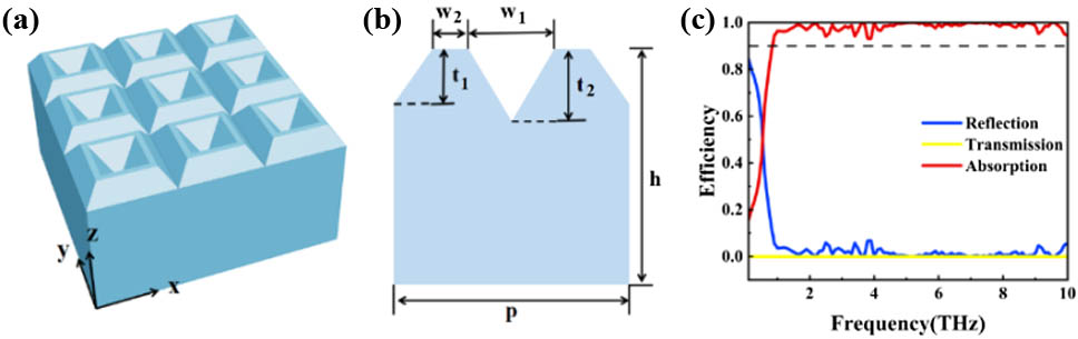
The schematic structural diagram of the terahertz metamaterial broadband absorber designed herein is shown in Fig. 1(a). Figure 1(b) is a schematic diagram of the element structure, wherein the structural parameters are μ, μ, μ, μ, μ, and μ.
Figure 1.(a) and (b) are schematics of arrays and element structures, respectively. (c) Absorption rate, reflectivity, and transmittance of metamaterial absorbers.
In numerical simulations, the dielectric constant of doped silicon is usually described by the Drude model [62], where is the dielectric constant of the intrinsic silicon, the is the Drude collision frequency, and the is the plasma frequency. is the doped concentration of silicon, is the amount of electron charge, is the vacuum dielectric constant, is the effective mass of the carrier in the doped silicon, and is the free-electron mass. When the carrier concentration of doped silicon and , the conductivity of the doped silicon is .
In order to optimize the design of the metamaterial absorber, the reflectivity (R) and transmittance (T) of the absorber are obtained by time-domain finite-difference method simulation, and the absorption rate of the absorber is calculated by equation [63–79]. In the simulation setup, periodic boundary conditions are used in the and directions and perfectly matched layers (PMLs) are used in the direction.
According to the structural parameters and settings above, the silicon-based metamaterial absorber is simulated and verified. Figure 1(c) is a simulation diagram of the R, T, and absorption rate of the all-medium metamaterial absorber; the absorber designed herein can achieve greater than 90% absorption in the range of 0.8–10 THz and can even achieve approximately 100% “perfect absorption” in the wideband range, achieving the design goal of ultrawideband in the terahertz band. Table 1 compares this paper with the published metamaterial absorber, and the structure designed in this paper has obvious advantages in the broadband, tunable, and production process.
Comparison Table of Different Types of All-Media Absorbers
References
Structure
Material
Absorption Band ()
Switchable
Etching Process
[77]
Square silicon ring
Silicon
0.5–5.7 THz
No
No experimental validation
[69]
H-shaped
Silicon
0.59–1.49 THz
Yes
Dry etching
[78]
Rings and cylindrical disks
Silicon
0.95–2 THz
Yes
Dry etching
[44]
Double-layer binary gratings
Silicon, SU-8
0.44–10 THz
No
Dry etching
[79]
Binary grating
Silicon, SU-8
0.3–3 THz
No
No experimental validation
This work
Square silicon ring
Silicon
0.8–10 THz
Yes
Wet etching
In order to analyze the contribution of each component to ultrawideband wave absorption, we simulated the absorption effect of the substrate without structure, the inverted pyramid structure, the quadrangle structure, and the ring structure on the 300 μm substrate. Figure 2(a) shows the absorption characteristics of a flat substrate to terahertz waves, and the bare substrate does not produce high absorption due to the mismatch between silicon wafers without any structure and free-space impedance. Figure 2(b) is a simulation diagram of the quadrangle structure; although the effect of broadband absorption can be achieved, only about 90% of the absorption can be achieved in the narrowband before 1.1 THz. Figure 2 (c) is the absorption efficiency of the inverted pyramid structure, which does not reach more than 90% in the range of 0.1–3 THz, but has an absorption rate of about 80% after 0.93 THz. Therefore, as shown in Fig. 2(d), the two structures are combined so that the impedance of the entire metamaterial matches the impedance of the free space, which increases the bandwidth and also improves the absorption efficiency.
Figure 2.(a) Absorption of terahertz waves by the substrate; (b) absorption of terahertz waves by the quadrangle structure; (c) absorption of terahertz waves by inverted pyramid structures; (d) absorption of terahertz waves by the combination of a quadrangle in a pyramidal structure.
Obviously, we can explain wideband absorption from the propagation characteristics of electromagnetic waves in inverted pyramidal and V-shaped cavities [63], but the absorption mechanisms at low and high frequencies are not the same. Therefore, in order to further understand the physical mechanism of the metamaterial broadband absorber designed in this paper, we plotted the electromagnetic field distribution at 0.8, 1.5, and 2.4 THz under the current incidence of TE polarization (electric field parallel to the axis) electromagnetic waves, with the red arrow as the average power flow. At 0.8 and 1.5 THz, the cavity structure is first matched to the free-space impedance, and the incoming electromagnetic waves smoothly enter the high-loss substrate from both sides of the ring structure, as shown by the red arrow in Figs. 3(a) and 3(c). Second, the two sides of the ring structure generate magnetic resonance under the action of terahertz waves, and the introduction of resonance makes the absorption bandwidth wider while increasing the absorption, as shown in Figs. 3(b) and 3(d). At 2.4 THz, the sidewall tilt angle of the ring structure is greater than 45°, which causes the sidewall of the cavity not to reflect the incident electromagnetic wave in reverse, but to reflect it downward along the cavity; finally, the incident wave undergoes multiple reflections into the doped silicon and is depleted. In addition, we also studied the transmission diffraction efficiency at μ, and the incident electromagnetic waves were diffracted to different orders and then absorbed by doped silicon. At the same time, it can be seen from Fig. 3(g) that there is absorption jitter in the high-frequency band. This is because our thickness h at this time is only 150 μm, and the incident electromagnetic wave generates Fabry–Pérot (F–P) resonance inside the structure, which causes jitter.
Figure 3.(a), (c), (e) Distribution of electric fields and time-averaged power flow (red arrows) in the plane; (b), (d), (f) magnetic field distribution and time-averaged power flow diagram in the yoz plane (red arrow); (g) is a diffraction efficiency (DE) plot in the range of 0.1–3 THz.
In practice, the direction of the electromagnetic wave incidence is uncertain. This requires that the metamaterial absorber we designed can also have excellent performance at a wide angle. Figures 4(a) and 4(b) show the absorption spectra of 0°–70° under TE and TM polarization conditions, respectively. As can be seen in Fig. 4(a), the absorption rate after the frequency point of about 1 THz decreases with the increase of the incidence angle, but the absorption rate before 1 THz jumps at an incident angle of 40°, because as the incidence angle increases, the magnetic resonance also increases, resulting in increased absorption. In Fig. 4(b), under TM incidence conditions, the absorption rate decreases with the increase of the incidence angle. Although the absorption rate of TM polarization at large-angle incidence is not as good as that of TE polarization, wideband absorption at wide angles is achieved in both polarization cases.
Figure 4.(a) and (b) are absorption spectra of different incident angles in TE and TM modes, respectively.
In order to explore the effects of structural parameters on absorption performance, the effects of t1, t2, w1, and w2 on the absorption spectrum were studied and plotted, as shown in Fig. 5. As can be concluded from Figs. 5(a) and 5(b), changing t2 and w1 does not have a great impact on the absorption rate because the high absorption in the low-frequency band is mainly caused by the external cavity of the ring structure. The absorption rate of the quadrangle structure in Fig. 2(b) also indicates that the contribution of the center inverted cone structure is small. When changing the size of t1, the absorption peak is redshifted with the increase of t1, and at μ, the absorption can be achieved in the broadband range of 0.58–10 THz above 90% because the increase of t1 makes it easier to couple low-frequency electromagnetic waves into doped silicon, reducing reflection. When the parameters are scanned for w2, it can be seen that the absorption increases as a function of incident frequency. This is because when t1 is constant, the increase of w2 makes the inclination angle of the sidewall of the annular cavity larger, and the incident wave is more easily coupled into the doped silicon.
Figure 5.Absorption spectra of different structural parameters.
Semiconductors in a thermal equilibrium state have a certain carrier concentration at a certain temperature [64]. This thermal equilibrium state downloads the flow subconcentration known as the equilibrium carrier concentration [65]. When we apply external effects to semiconductors, such as changing temperature, illumination, or applying voltage, we will destroy the conditions of thermal equilibrium and cause it to deviate from the thermal equilibrium state, which is called the nonequilibrium state. The concentration of carriers in nonequilibrium semiconductors will be more than the concentration of equilibrium carriers, and these additional carriers are called unbalanced carriers or excess carriers.
At a certain temperature, when we use light of an appropriate wavelength to irradiate doped silicon, as long as the energy of the photon is greater than the bandgap width of the semiconductor, then the photon can excite the valence band electrons to the guide band, resulting in an electron-hole pair [66]. Light injection by an unbalanced carrier causes the conductivity of the semiconductor to increase, which changes the electromagnetic properties of the semiconductor. When we stop illumination, the valence band electrons cannot be excited to the conduction band and the electrons that were originally excited to the conduction band return to the valence band, the nonequilibrium carrier disappears, and the semiconductor returns to equilibrium. It has been shown that the generation and disappearance of nonequilibrium carriers often require only the order of microseconds or nanoseconds.
According to the Beer–Lambert law, the incident flux on the surface of the silicon wafer varies with depth under 800 nm pump light illumination in accordance with the formula: , wherein the is the flux at depth , the is the proportion coefficient independent of the light intensity, also known as the absorption coefficient of pumped light, and [67,68]. Assuming that all incident light is converted into in-semiconductor unbalanced carriers and is uniform, the distribution of carrier concentrations in silicon in the direction is formulated as [69] where () is the energy of the incident pump light. Figures 6(a) and 6(b) show the distribution of doped silicon carrier concentration and plasma frequency with depth under pumped light at μ energy, and it can be seen that even small light can cause a large change in carrier concentration, thereby changing the electromagnetic material properties of doped silicon.
Figure 6.(a) and (b) show the relationship between the doped silicon carrier concentration and the plasma frequency and the depth z under different pump lights, respectively.
In the numerical simulation, we have to discretize the carrier concentrations that vary continuously in space, as shown in Fig. 6(a). In order to be closer to the actual situation, the gradient of carrier concentration change should not be too large. Therefore, we divide the metamaterial structure with a depth of 50 μm into ten layers, each with a thickness of 5 μm, as shown in Fig. 7. We approximate the carrier concentrations of each layer to obtain a carrier concentration distribution map that matches the metamaterial structure.
Figure 7.Calculated carrier concentration (curve) approximated to the carrier concentration in the hierarchical model (histogram).
In order to simulate and verify the tunable properties of the metamaterial designed in this paper, we simulated the absorption rate change plot in the range of 0.1–1.2 THz with an incident angle of 10°, as shown in Fig. 8(a). As the pump light energy increases, it is indeed possible to adjust the absorption performance. In order to be able to more intuitively and clearly study the performance of the tunable absorber we designed, we introduce the modulation depth,
Figure 8.(a) Absorption spectra under pump light regulation of different energy densities; (b) modulation depth at two frequency points of 0.8 and 1.1 THz.
and represent the maximum and minimum values of light absorption under different incident pumps. We plotted the change in modulation depth at the two absorption peaks of 0.8 and 1.1 THz according to Eq. (3). As shown in Fig. 8(b), for 0.8 THz, as the pump light energy increases, the absorption rate decreases sharply, and the modulation depth reaches a maximum at μ, which is 77%. For 1.1 THz, the modulation depth also reaches 71%, which meets our requirements for tunable devices. This may be due to the fact that regions of high carrier density are completely shielded from electromagnetic waves, which cannot pass through the structure into the material and are converted into other modes and reflected back, while low carrier concentrations allow electromagnetic waves to propagate and dissipate [69]. However, in the 0.8–1.1 THz band, with the increase of incident pump light, the absorption rate changes nonlinearly, the position of the absorption peak also changes, and the absorption peak appears at 0.8 THz under the excitation of μ pump light. This is due to the fact that the structure produces a strong diffraction on the incident electromagnetic waves, and the change in the refractive index of the dielectric material leads to an offset in the position of the diffraction peak.
C. Experimental Preparation and Testing
In order to verify the actual performance of the ultrawideband absorber we designed, this paper uses lithography and etching to produce cycle structures on silicon wafers. The resistivity of doped silicon used in the manufacture of broadband absorbers is . Figure 9 draws a production flow diagram of the ultrawideband absorber designed in this paper: (1) cleaning, oxidation; (2) uniformly coated photoresist; (3) exposure (contact exposure technology is used in exposure, which can greatly reduce errors caused by lithography), and development; (4) etched silica; (5) degluing; (6) etched silicon; (7) removal of the silica mask.
Figure 9.Flow chart of the production of the absorber.
In the above process, there is a serious convex angle cutting phenomenon in the anisotropic wet corrosion of step (7). Due to the presence of convex angle corrosion, when the Si(100) table surface is corroded, there will be a serious cutting phenomenon at the convex angle, resulting in a change in structural properties. Therefore, it is necessary to protect the convex angle.
In previous studies, changing the type and concentration of the corrosive fluid can reduce the occurrence of convex angle cutting to a certain extent [70–72], but this method will fail when the corrosive structure has a certain depth. By adding surfactants, such as IPA and Triton x-100, the convex angle cutting can be suppressed, but its effect is also limited. In the manufacturing process, predictable defects can theoretically be compensated in advance [73], so adding a specific compensation structure to the convex angle of the structure allows it to be consumed during the etching process, thus directly protecting the structure we designed. In past studies, researchers have usually added compensating triangles, squares, or bars to the convex angles [74,75], although these structures can obtain better compensation effects according to certain theoretical designs, but often need to occupy a large space. The spacing between the four right-angle structures applied to the structure we designed is difficult to meet.
Therefore, we use a bar compensation structure. The single-strip compensation structure shown in Fig. 10(a) begins with a tangential effect from C and D during corrosion, resulting in two corrosion lines direction. However, as the drilling deepens, it will inevitably corrode the triangular area surrounded by ABC. To solve this problem, we add a branch vertically, as shown in Fig. 10(b). Convex corrosion starts at the same time by the free ends F and D, E, but the corrosion starting from point F preferentially reaches point C, so that it does not cause the cutting effect of Fig. 10(a), but the effective length of this L-shaped compensation structure is too short. As shown in Fig. 10(c), the L-shaped structure is changed to a T-shaped structure, and the length of the T-shaped left horizontal bar is smaller than that on the right. The compensatory structure of this design begins to corrode at the convex angle by the four free ends of H, I, E, and D when corrosion occurs, and the left side of the T-shaped structure will reach the center bar before the right side, which not only lengthens the effective length of the compensation structure but also avoids the cutting effect of Fig. 10(a). In the structure we designed, the length on the right side of the T-shaped compensation structure cannot be greater than 50 μm, which greatly reduces the effective length of the compensation structure. Therefore, in the comprehensive design principle and structural dimensions, the strip compensation structure shown in Fig. 10(d) is designed, wherein μ, μ, and μ. Although the case of appears in Fig. 10(d), L2 can be regarded as infinitely long in the periodic structure shown in Fig. 10(e), so that the overall effective length is greatly increased by the complementary design of each structure, and the longer compensation structure can adapt to different types of corrosive liquids.
Figure 11 shows the corrosion process diagram of the structure. As shown in Fig. 11(a), first of all, a 33% potassium hydroxide solution was used to corrode for 30 min at 80°C, and an appropriate amount of IPA solution was added to the corrosion solution. Potassium hydroxide corrosion fluids are used to quickly release structures and shorten corrosion time, and IPA is added to smooth the etched surfaces [76]. Next, replace the potassium hydroxide solution with a 25% tetramethyl ammonium hydroxide solution (TMAH) and add 3 mL of IPA solution to the 20 mL TMAH to ensure a smooth etching structure. Theoretically, potassium hydroxide could continue to be used as a corrosion solution, but the selection ratio of potassium hydroxide to silicon and silica was too small [77], resulting in silica being completely corroded before it had corroded to the required depth, so the TMAH solution with a larger selection ratio was used instead. Figure 11(b) is a structural diagram of 1 h continuous corrosion at 80°C. Most of the compensatory structures are corroded and reach the predetermined corrosion depth, but there are still structural remains at the junction of the four structures. Finally, the TMAH solution with Triton x-100 added to it corrodes for 1 h at a 70°C water bath, with the aim of using the small cutting effect on the convex angle under this ratio to achieve the removal of the remaining structure. Figure 11(c) is the final corrosion result figure; the structure is angular, there is no tangential angle, the surface is smooth, and the structure is complete.
Figure 11.(a) KOH IPA corrosion for 30 min; (b) TMAH IPA corrosion for 60 min; (c) TMAH Triton x-100 corrosion for 60 min.
To test the depth of the sample prepared by the experiment, the sample in Fig. 12(a) was measured using a profiler, with a V-shaped groove corrosion depth of approximately 79 μm and an inverted pyramid corrosion depth of approximately 87 μm, as shown in Fig. 12(b). There is an error in the test process. If the probe of the step meter does not walk along the lowest point of the structure, it will make the measured depth inaccurate. The sample was tested using a terahertz time-domain spectrometer (THz-TDS), and the test data were processed and plotted together with the simulation data in Fig. 12(c), from which it can be seen that the experiment and the simulation curve trend are the same. However, the absorption rate of the actual test is slightly lower than the simulated absorption rate; on the one hand, the doped concentration of the silicon used in the simulation is lower than the doped concentration of the actual silicon used, resulting in a blueshift of the absorption peak, and on the other hand, there are unavoidable errors in both the preparation and testing.
Figure 12.(a) Physical view of a metamaterial absorber; (b) step meter measured depth map; (c) simulation and experimental testing of absorption rates.
3. MICROFLOW CHANNEL SENSOR BASED ON METAMATERIAL ABSORBER
A. Microflow Channel Sensor
As can be seen from Fig. 8(a), when the concentration of doped silicon increases, a sharp absorption peak can be generated in the range of 0.6–1.2 THz. This makes the metamaterial absorber we designed promising for use in sensors. We introduce refractive index frequency sensitivity (S), quality factor (Q) and figure of merit (FOM) descriptions,
Among them, is the amount of refractive index change, is the amount of absorption peak movement caused by the change of , FWHM is the width of the curve at half of the absorption peak, and is the frequency point where the absorption peak is located.
Many biomolecules have refractive indices in the range of 1.0–1.8, so we simulated absorption spectra at different refractive indices on heavily doped silicon with a resistivity of . Figure 13(a) shows the analyte to be measured adsorbed on the metamaterial in a coated manner, and we analyzed the sensor performance of the 1 μm, 3 μm, and 5 μm thicknesses of the substance to be measured, respectively. Figure 13(b) shows the absorption spectra of the substance to be measured at 5 μm, and it can be seen that as the refractive index of the substance to be measured increases, the absorption peaks are significantly redshifted. In order to visualize the influence of refractive index and thickness on frequency movement, the resonant frequency at different thicknesses is plotted in Fig. 13(c) with the refractive index of the substance to be measured, and it can be seen that when the film thickness of the substance to be measured is less than 5 μm, the frequency movement is nonlinear, and the sensitivity and FOM values are very low; when the thickness of the substance to be measured is 5 μm, the frequency offset is approximately linear, and the S reaches 17.5 GHz/RIU, , .
Figure 13.(a) Schematic diagram of the material to be measured coated on the surface of the metamaterial; (b) refractive index detection characteristics of the sensor; (b) refractive index detection characteristics of the sensor under different thicknesses of the substance to be measured.
It can be seen that the doped silicon metamaterial absorber can realize the detection of the substance to be measured at different refractive indices. However, we can see from its refractive index and FOM value that the sensing performance of the sensor is limited. This is because the resonant electromagnetic field of the sensor is mainly bound in the void of the structure, only the edge field is in contact with the analyte to be measured, and the strength of the edge field directly determines the sensitivity of the sensor.
Figure 14.(a) Integrated microflow channel sensor based on a metamaterial absorber; (b) relationship between the absorption peak of the microflow channel sensor and the refractive index.
To explore the effect of the height h1 of the microchannel and the thickness of the top cover h2 and refractive index on the sensing performance, we simulated the effect of various parameters on the performance of the sensor. First of all, we studied the effect of the height h1 of the microflow channel and the refractive index of the substance to be measured on the absorption peak displacement, and it can be seen from Fig. 15(a) that when the thickness of the substance to be measured gradually increases, the absorption peak displacement also increases. However, the substance to be measured in the actual detection will have a high absorption of terahertz waves, and the thinner the substance to be measured, the less effect there is on the peak amplitude of absorption. Therefore, the thickness of the microflow channel h1 is 50 μm, taking into account the sensitivity while ensuring a large absorption amplitude. Second, we studied the effect of cap thickness h2 on sensor performance and found that the top cover thickness h2 hardly affected the performance of the sensor, as shown in Fig. 15(b). Finally, we studied the effect of the refractive index of the cap on the sensing performance and found that when the refractive index of the top cover becomes larger, it will lead to many spurious absorption peaks near the main peak, and the Q value and sensitivity S are significantly reduced, as shown in Fig. 15(c).
Figure 15.(a) At different channel thicknesses h1, the relationship between the absorption peak and the refractive index n of the analyte; (b) relationship between the absorption peak and the refractive index n of the analyte at different top cover thicknesses h2; (c) relationship between the absorption peak and the refractive index n of the analyte under different cap refractive indices .
The preparation process of the integrated microflow channel sensor based on the metamaterial absorber is shown in Fig. 16(a), wherein we (1) prepare the microflow channel substrate; (2) prepare the top cover and punch the holes; and (3) install the steel needle and seal it. The preparation method of the metamaterial structure before process (1) is consistent with Fig. 9. Figure 16(b) shows a physical diagram of the microflow channel sensor, and the acrylic glass fixture is designed to avoid leakage and fix the steel needle.
Figure 16.(a) Microflow channel sensor preparation flow chart; (b) physical drawing of the microflow channel sensor.
The detection effect of the microflow channel was subsequently verified using a reflective terahertz time-domain spectrometer. As shown in Fig. 17, we test the reflected spectra of terahertz waves by the microflow channel when entering air, alcohol (), and water (). During the experimental test, the terahertz wave was normally incident on the metamaterial, and the direction of the electric field was parallel to the axis in Fig. 1(a). What we have designed is an absorber type sensor, so we can calculate the absorption rate using the formula . The test curve of the air in Figs. 17(a) and 17(d) differs significantly from the simulation curve, possibly because we are not passing through dry air, and the moisture in the air absorbs a large number of terahertz waves and causes a change in peak position. Figures 17(b) and 17(e) are the test spectra of alcohol. It can be seen that there is a certain frequency shift in the experimental and simulation results, which may be caused by the difference between the dielectric constant of alcohol and the actual one. The sample water tested in Figs. 17(c) and 17(f) is a strongly polar molecule with strong absorption of terahertz waves, resulting in insignificant peak changes in the test or simulation. If water is used as a biomolecular carrier, the height of the microfluidic channel needs to be reduced, which can minimize the thickness of the water, reduce the absorption of terahertz waves, and improve the resolution. Our proposed sensor may be applied to other areas [80–87].
Figure 17.(a), (b), and (c) are the simulated (black) and test (red) reflectance plots for air, alcohol, and water, respectively; (d), (e), and (f) are the simulated (black) and test (red) absorbance plots for air, alcohol, and water, respectively.
We designed and prepared an ultrawideband and wide-angle metamaterial absorber based on silicon, which achieves an absorption effect greater than 90% in the range of 0.8–10 THz by combining the quadrangular structure with the inverted pyramid structure. Combined with the electromagnetic field diagram and energy loss at the absorption peak, the physical mechanism for achieving broadband absorption is analyzed. Semiconductor materials were used to generate excess carriers under specific wavelength light excitation conditions, and the dynamic regulation of the absorption amplitude of metamaterial absorbers was realized so that broadband absorption and narrowband absorption can be switched at will. In addition, in order to broaden the practical application of the metamaterial absorber, the absorption peak with a high Q is realized without changing the structural parameters, and combined with the microflow channel detection, the high-sensitivity sensor was designed and realized. Finally, the preparation of metamaterial absorber and microfluidic sensor was discussed, and the compensation structure in wet corrosion was designed by using the compensation principle, which solves the problem of convex angle cutting in the wet corrosion process. The ultrawideband absorbent material proposed in this paper has a wide angle, is easy to make, has the same preparation process as the complementary metal oxide semiconductor (COMS) process, and is easy to integrate and to miniaturize. Electromagnetic stealth, terahertz imaging and sensing, and other fields are potential application prospects.
[52] L. Yue, Y. Wang, Z. Cui, X. Zhang, Y. Zhu, C. Yang, X. Wang, S. Chen. Highly sensitive detection of optical tunable terahertz multi-band absorber based on all-dielectric grating. 45th International Conference on Infrared, Millimeter, and Terahertz Waves (IRMMW-THz), 1-2(2020).
[58] S. Yin, W. Huang, L. Guo. Terahertz metamaterial sensor integrated with microfluidic channel. Cross Strait Quad-Regional Radio Science and Wireless Technology Conference (CSQRWC), 1-2(2019).
[71] V. Jovic, J. Lamovec, M. Popovic. Investigation of silicon anisotropic etching in alkaline solutions with propanol addition. 26th International Conference on Microelectronics, 355-358(2008).
[72] T. P. Kuehn, S. M. Ali, S. C. Mantell, E. K. Longmire. Reliability, Packaging, Testing, and Characterization of MEMS/MOEMS VI, 196(2007).
[73] N. Marenco, W. Reinert, S. Warnat, P. Lange, S. Gruenzig, G. Allegato, G. Hillmann, H. Kostner, W. Gal, S. Guadagnuolo, A. Conte, K. Malecki, K. Friedel. Investigation of key technologies for system-in-package Integration of inertial MEMS. Symposium on Design, Test, Integration & Packaging of MEMS/MOEMS, 35-40(2009).