• Laser & Optoelectronics Progress
  • Vol. 60, Issue 18, 1811001 (2023)
Hongbo Li1、2、3、4、5, Jingyin Xu4、5, Wenyin Wei4、5, En'en Li1、2、3、4、5, Kai Zhang4、5, Hong Li4、5, Yirong Wu1、2、3、4、5, Tianwu Wang1、2、3、4、5、*, and Guangyou Fang1、2、3、4、5、**
Author Affiliations
  • 1Aerospace Information Research Institute, Chinese Academy of Sciences, Beijing 100094, China
  • 2Key Laboratory of Electromagnetic Radiation and Sensing Technology, Chinese Academy of Sciences, Beijing 100190, China
  • 3School of Electronic, Electrical and Communication Engineering, University of Chinese Academy of Sciences, Beijing 100049, China
  • 4Greater Bay Area Branch of Aerospace Information Research Institute, Chinese Academy of Sciences, Guangzhou 510700, Guangdong, China
  • 5Guangdong Provincial Key Laboratory of Terahertz Quantum Electromagnetics, Guangzhou 510700, Guangdong, China
  • show less
    DOI: 10.3788/LOP231383 Cite this Article Set citation alerts
    Hongbo Li, Jingyin Xu, Wenyin Wei, En'en Li, Kai Zhang, Hong Li, Yirong Wu, Tianwu Wang, Guangyou Fang. Progress of High Spatiotemporal Resolution Terahertz Scanning Tunneling Microscope for Near-Field Imaging[J]. Laser & Optoelectronics Progress, 2023, 60(18): 1811001 Copy Citation Text show less
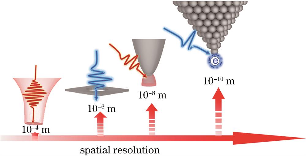
    Development of near-field super-resolution imaging techniques
    Fig. 1. Development of near-field super-resolution imaging techniques
    Diffusion of Si-adatom dimers[22]. (a) (b) Diffusion of Si-adatom dimers at a temperature of 65 ℃; (c) (d) observation of Si dimer captured by substrate defects at different scales of 70 Å and 90 Å, respectively
    Fig. 2. Diffusion of Si-adatom dimers[22]. (a) (b) Diffusion of Si-adatom dimers at a temperature of 65 ℃; (c) (d) observation of Si dimer captured by substrate defects at different scales of 70 Å and 90 Å, respectively
    Conceptual diagram of photoconductive-gated STM and junction-mixing STM. (a) Optical path of pump light and probe light illuminating the sample and tip with a certain time delay, utilizing photoconductive bias to control the tunneling current[24]; (b) optical path of two laser beams simultaneously illuminating the sample end with a certain optical path difference, exciting picosecond pulse voltage[26]
    Fig. 3. Conceptual diagram of photoconductive-gated STM and junction-mixing STM. (a) Optical path of pump light and probe light illuminating the sample and tip with a certain time delay, utilizing photoconductive bias to control the tunneling current[24]; (b) optical path of two laser beams simultaneously illuminating the sample end with a certain optical path difference, exciting picosecond pulse voltage[26]
    Direct coupling optical experiment and its thermal analysis. (a) Experiment operated by Hamers et al.[31]; (b) relationship between chopping frequency and thermal expansion effect[32]
    Fig. 4. Direct coupling optical experiment and its thermal analysis. (a) Experiment operated by Hamers et al.[31]; (b) relationship between chopping frequency and thermal expansion effect[32]
    Diagram of the SPPX-STM method and its current modulation principle. (a) Experiment operated by Takeuchi et al.[34]; (b) symmetrical current peak generated by autocorrelation scanning laser[34]; (c) case of delayed sinusoidal modulation[34]; (d) case of delayed square wave modulation[35]
    Fig. 5. Diagram of the SPPX-STM method and its current modulation principle. (a) Experiment operated by Takeuchi et al.[34]; (b) symmetrical current peak generated by autocorrelation scanning laser[34]; (c) case of delayed sinusoidal modulation[34]; (d) case of delayed square wave modulation[35]
    Exploring carrier dynamics in GaAs-PIN junction structures using the SPPX-STM method[72]. (a) Conceptual diagram of heterojunction; (b) energy band diagram; (c) time-resolved carrier diffusion diagram
    Fig. 6. Exploring carrier dynamics in GaAs-PIN junction structures using the SPPX-STM method[72]. (a) Conceptual diagram of heterojunction; (b) energy band diagram; (c) time-resolved carrier diffusion diagram
    Introduction to the basic characteristics and principles of THz-STM. (a) Tip coupled with THz[6]; (b) I-V curve of the STM tunneling junction under the influence of THz in a biased form[6]; (c) (d) thermal effect of THz[86]; (e) enhancement of field intensity due to the tip antenna effect[82]; (f) Keldysh model considering the transition probability of Volkov states scattered by needle point electronic states into air[85]
    Fig. 7. Introduction to the basic characteristics and principles of THz-STM. (a) Tip coupled with THz[6]; (b) I-V curve of the STM tunneling junction under the influence of THz in a biased form[6]; (c) (d) thermal effect of THz[86]; (e) enhancement of field intensity due to the tip antenna effect[82]; (f) Keldysh model considering the transition probability of Volkov states scattered by needle point electronic states into air[85]
    Model of tunneling current in THz-STM and influence of polarization and carrier phase. (a) THz response observed for polarization perpendicular to the tip[86]; (b) current responses of THz under various carrier phase conditions[87]; (c) Bardeen model considering the metal surface[83]; (d) THz peak current and rectified current[83]; (e) schematic of THz carrier envelope phase shifter[89]
    Fig. 8. Model of tunneling current in THz-STM and influence of polarization and carrier phase. (a) THz response observed for polarization perpendicular to the tip[86]; (b) current responses of THz under various carrier phase conditions[87]; (c) Bardeen model considering the metal surface[83]; (d) THz peak current and rectified current[83]; (e) schematic of THz carrier envelope phase shifter[89]
    Source of THz-STM rectification current signal[6]. (a) Transient current pulse of 100-500 fs generated by a THz transient bias voltage of up to 10 V magnitude; (b) transient current pulse rectified by a pre current amplifier and chopping modulation
    Fig. 9. Source of THz-STM rectification current signal[6]. (a) Transient current pulse of 100-500 fs generated by a THz transient bias voltage of up to 10 V magnitude; (b) transient current pulse rectified by a pre current amplifier and chopping modulation
    THz-STM time resolution capability[86]. (a) THz autocorrelation pulse pairs acting on the STM needle tip; (b) increasing the peak electric field intensity of THz, there is a growth threshold in the tunneling current variation curve caused by THz on Au nanoislands and HOPG samples; (c) increasing the peak electric field intensity of THz results in changes in the full width at half maximum of THz autocorrelation peaks on both samples; (d) (e) amplitude and full width at half maximum of THz autocorrelation peaks on two samples as a function of THz electric field intensity
    Fig. 10. THz-STM time resolution capability[86]. (a) THz autocorrelation pulse pairs acting on the STM needle tip; (b) increasing the peak electric field intensity of THz, there is a growth threshold in the tunneling current variation curve caused by THz on Au nanoislands and HOPG samples; (c) increasing the peak electric field intensity of THz results in changes in the full width at half maximum of THz autocorrelation peaks on both samples; (d) (e) amplitude and full width at half maximum of THz autocorrelation peaks on two samples as a function of THz electric field intensity
    Steady state imaging of THz-STM on various samples. (a) Nanoresolution imaging of Au nanoislands on HOPG[6]; (b) THz constant height mode imaging of armchair graphene strips grown on Au111[60]; (c) imaging of THz-STM on Si111 is shown in the left image with THz driven scanning (40 nm×40 nm), the built-in image shows amplification of a specific area (8.5 nm×8.5 nm), and the right image shows the height difference between STM imaging and THz driven imaging within the red line range[58]; (d) imaging of THz-STM using phase-locked amplification mode on metal Cu111[83]
    Fig. 11. Steady state imaging of THz-STM on various samples. (a) Nanoresolution imaging of Au nanoislands on HOPG[6]; (b) THz constant height mode imaging of armchair graphene strips grown on Au111[60]; (c) imaging of THz-STM on Si111 is shown in the left image with THz driven scanning (40 nm×40 nm), the built-in image shows amplification of a specific area (8.5 nm×8.5 nm), and the right image shows the height difference between STM imaging and THz driven imaging within the red line range[58]; (d) imaging of THz-STM using phase-locked amplification mode on metal Cu111[83]
    Field-induced fluorescence effect in THz-STM[94]. (a) Morphology of Au islands on Ag111; (b) fluorescence differences at the ends and sides of Au islands; (c) imaging for Au islands through fluorescence differences
    Fig. 12. Field-induced fluorescence effect in THz-STM[94]. (a) Morphology of Au islands on Ag111; (b) fluorescence differences at the ends and sides of Au islands; (c) imaging for Au islands through fluorescence differences
    Single-point pump-probe detection experiment in THz-STM. (a) SEM image of InAs quantum dots grown on Au111[6]; (b) THz detection of the charging and discharging process of InAs quantum dots under 800 nm infrared light pumping[6]; (c) STM scanning of 2H-MoTe2 bulk material[62]; (d) experiment involving 1030-nm pumping and THz detection[62]; (e) schematic of the pumping and detection process[62]; (f) pumping and detection curves under varying pump intensities[62]
    Fig. 13. Single-point pump-probe detection experiment in THz-STM. (a) SEM image of InAs quantum dots grown on Au111[6]; (b) THz detection of the charging and discharging process of InAs quantum dots under 800 nm infrared light pumping[6]; (c) STM scanning of 2H-MoTe2 bulk material[62]; (d) experiment involving 1030-nm pumping and THz detection[62]; (e) schematic of the pumping and detection process[62]; (f) pumping and detection curves under varying pump intensities[62]
    High spatio-temporal resolution scanning in THz-STM. (a) Discharge process of InAs quantum dots on Au[6]; (b) longitudinal diffusion process of hot carriers on Au in C60[95]
    Fig. 14. High spatio-temporal resolution scanning in THz-STM. (a) Discharge process of InAs quantum dots on Au[6]; (b) longitudinal diffusion process of hot carriers on Au in C60[95]
    MethodSpatial resolution /nmTime resolutionReference
    High-speed STM0.1ms2163-64
    Atom-tracking STM0.1ms22
    It)curve0.1μs23
    PG-STM202 ps24-25
    JM-STM110 ps26-286877
    All electronic pump-probe STM0.11 ns18
    SPPX-STM0.1200 fs34-35377173-76
    THz-STM0.1100 fs658-5961-6278-79
    Table 1. Development of time-resolved STM
    Hongbo Li, Jingyin Xu, Wenyin Wei, En'en Li, Kai Zhang, Hong Li, Yirong Wu, Tianwu Wang, Guangyou Fang. Progress of High Spatiotemporal Resolution Terahertz Scanning Tunneling Microscope for Near-Field Imaging[J]. Laser & Optoelectronics Progress, 2023, 60(18): 1811001
    Download Citation