• Photonics Research
  • Vol. 7, Issue 6, 659 (2019)
Zhi Liu1、2, Jiashun Zhang1, Xiuli Li1、2, Liangliang Wang1, Jianguang Li1, Chunlai Xue1、2, Junming An1、2, and Buwen Cheng1、2、*
Author Affiliations
  • 1State Key Laboratory on Integrated Optoelectronics, Institute of Semiconductors, Chinese Academy of Sciences, Beijing 100083, China
  • 2Center of Materials Science and Optoelectronics Engineering, University of Chinese Academy of Sciences, Beijing 100049, China
  • show less
    DOI: 10.1364/PRJ.7.000659 Cite this Article Set citation alerts
    Zhi Liu, Jiashun Zhang, Xiuli Li, Liangliang Wang, Jianguang Li, Chunlai Xue, Junming An, Buwen Cheng. 25 × 50 Gbps wavelength division multiplexing silicon photonics receiver chip based on a silicon nanowire-arrayed waveguide grating[J]. Photonics Research, 2019, 7(6): 659 Copy Citation Text show less
    Top-view optical micrographs of the WDM receiver chip, AWG, and Ge-on-Si waveguide photodetector array.
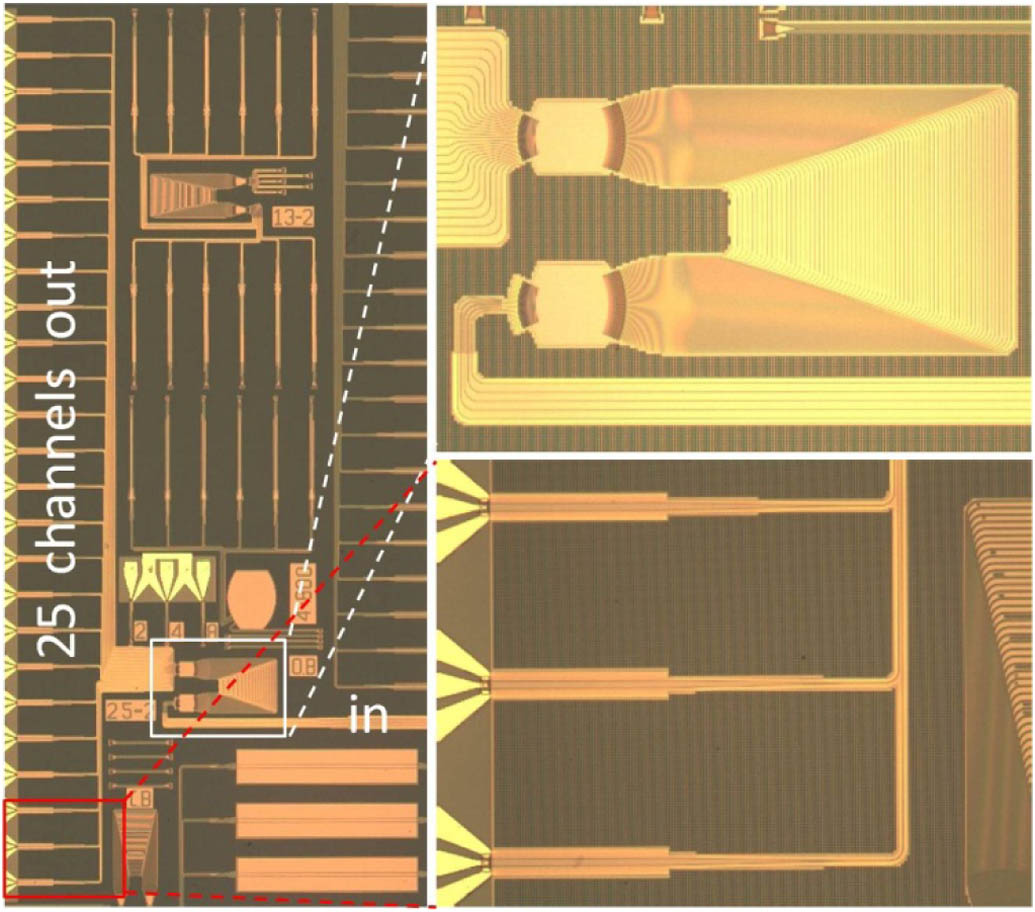
    Fig. 1. Top-view optical micrographs of the WDM receiver chip, AWG, and Ge-on-Si waveguide photodetector array.
    (a) Typical I-V curves of the standalone photodetector with/without light incidence (1550 nm) from 1 V to −3 V. The optical power entering the photodetector is about −9.4 dBm. The inset is a schematic of the optical coupling in this measurement. (b) Spectral responsivity of the standalone photodetector from 1530 to 1580 nm under −1 V.
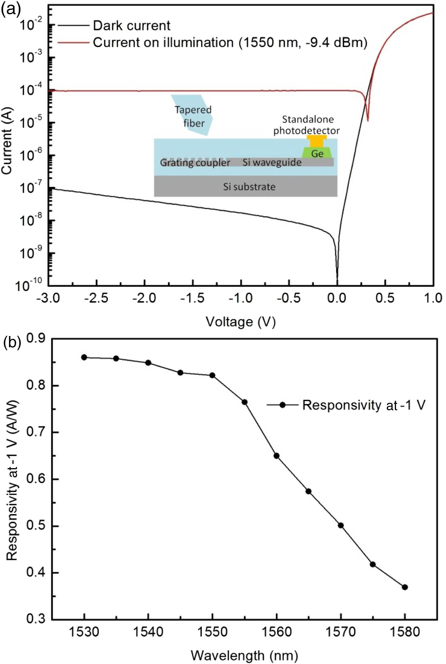
    Fig. 2. (a) Typical I-V curves of the standalone photodetector with/without light incidence (1550 nm) from 1 V to 3  V. The optical power entering the photodetector is about 9.4  dBm. The inset is a schematic of the optical coupling in this measurement. (b) Spectral responsivity of the standalone photodetector from 1530 to 1580 nm under 1  V.
    Frequency response of a standalone photodetector at various reverse biases.
    Fig. 3. Frequency response of a standalone photodetector at various reverse biases.
    (a) Photocurrent spectrum of each channel of the WDM receiver chip. The inset is a schematic of the optical coupling in this measurement. (b) Transmission spectra of the 25-channel 200 GHz AWG.
    Fig. 4. (a) Photocurrent spectrum of each channel of the WDM receiver chip. The inset is a schematic of the optical coupling in this measurement. (b) Transmission spectra of the 25-channel 200 GHz AWG.
    40 Gbps and 50 Gbps eye diagrams of channels 5, 10, 15, 20, and 25 at 0 and −1 V. The modulator eye diagrams are also shown for comparison.
    Fig. 5. 40 Gbps and 50 Gbps eye diagrams of channels 5, 10, 15, 20, and 25 at 0 and −1 V. The modulator eye diagrams are also shown for comparison.
    BER curves of channel 10 at 40 and 50 Gbps. The 40 and 50 Gbps eye diagrams of channel 10 under −2.4 and −2.2 dBm input optical power are shown for comparison.
    Fig. 6. BER curves of channel 10 at 40 and 50 Gbps. The 40 and 50 Gbps eye diagrams of channel 10 under 2.4 and 2.2  dBm input optical power are shown for comparison.
    DemultiplexerPlatformInsertion Loss (dB)Cross Talk (dB)Number of ChannelsReceiving Bit Rate (Gbps)
    Echelle grating [6]3 μm SOI2–4<274025
    Microring [8]220 nm SOI0.3<20820
    AMI [10]220 nm SOI0.5<15412.5
    AWG [11]300 nm SOI1.5–4.5<183210
    This work: AWG220 nm SOI5–8<122550
    Table 1. Performance Comparison for Si Photonic WDM Receivers
    Zhi Liu, Jiashun Zhang, Xiuli Li, Liangliang Wang, Jianguang Li, Chunlai Xue, Junming An, Buwen Cheng. 25 × 50 Gbps wavelength division multiplexing silicon photonics receiver chip based on a silicon nanowire-arrayed waveguide grating[J]. Photonics Research, 2019, 7(6): 659
    Download Citation