Abstract
A high-performance monolithic integrated wavelength division multiplexing silicon (Si) photonics receiver chip is fabricated on a silicon-on-insulator platform. The receiver chip has a 25-channel Si nanowire-arrayed waveguide grating, and each channel is integrated with a high-speed waveguide Ge-on-Si photodetector. The central wavelength, optical insertion loss, and cross talk of the array waveguide grating are 1550.6?nm, 5–8?dB, and , respectively. The photodetectors show low dark current density of at and a high responsivity of 0.82?A/W at 1550?nm. High bandwidths of 23 and 29?GHz are achieved at 0 and , respectively. Each channel can operate at 50?Gbps with low input optical power even under zero bias, which realizes an aggregate data rate of 1.25?Tbps.1. INTRODUCTION
In past decades, demands for short-length optical communication with large capability and high speed have been increasing exponentially in modern data centers. Unfortunately, performance of single optical channel data transmission with one laser or detector is far from the necessary requirements. Therefore, parallel transmission is a feasible strategy to increase the capability and speed of optical communication. In different methods of parallel transmission, wavelength division multiplexing (WDM) technology is regarded as one of the best solutions. Due to high reliability and large transmission capability, the WDM technology has been rapidly developed and widely used in optical communication [1]. Using different wavelengths as different channels, WDM systems can transmit multiple channel data through a single fiber, which significantly increases the aggregate data rate. Thus, the transmission capability of the optical receiver can be increased sharply by using WDM technology. Common high-speed WDM receivers are mainly assembled from III–V photodetectors and demultiplexers such as thin-film filters and silica array waveguide gratings (AWGs). Compared to the former, monolithic integrated receivers have obvious advantages in size, cost, and reliability. Monolithic integrated 40-channel demultiplexers and Ge photodetector arrays on silicon (Si) have been reported [2]. Although the demultiplexer has better performance than its Si counterpart, an integrated demultiplexer with a Si waveguide is complex. Moreover, due to the relatively small refractive index of , the footprint of a demultiplexer is large, which is not the best choice for monolithic integrated WDM receivers.
Si photonics has the advantages of having a small footprint, high performance, low cost, and being highly compatible with Si complementary metal oxide semiconductor (CMOS) technology, which can provide a promising platform for integrating passive components and photoelectronic devices [3], such as high-speed photodetectors [4] and modulators [5]. Monolithic silicon-on-insulator (SOI)-based WDM-integrated receivers using Si demultiplexers, such as echelle gratings [6,7], microrings [8,9], and angled multimode interferometers (AMIs) [10] have been realized. Among them, the highest aggregate data rate of 1 Tbps has been demonstrated by using 40 channels, each operating at 25 Gbps [6]. However, Si AWG is regarded as an excellent candidate for WDM. Due to the high refractive index and working principle, the AWG has very small bend radius, compact footprint, and large output channels. Many SOI nanowire AWGs have been realized and used in monolithic Si photonic receivers [11–13]. But, due to the small tolerance in the fabrication process induced by high refractive contrast or low performance of the integrated photodetectors, the reported performance of the WDM receiver based on SOI nanowire AWG is not satisfactory [11].
In this work, we demonstrate a 25-channel monolithic integrated WDM Si photonics receiver chip with Si nanowire AWG. The 25-channel 200 GHz Si nanowire AWG exhibits an optical insertion loss of 5–8 dB, cross talk of , and a central wavelength of 1550.6 nm. The integrated Ge on Si waveguide photodetector not only has a low dark current density and high responsivity, but also can operate at the high speed of 50 Gbps. The overall fiber-accessed responsivity and total aggregate transmission of the WDM receiver chip are 0.09–0.24 A/W and 1.25 Tbps, respectively.
Sign up for Photonics Research TOC. Get the latest issue of Photonics Research delivered right to you!Sign up now
2. MATERIAL GROWTH AND DEVICE FABRICATION
The AWGs were fabricated on an SOI substrate with a 220-nm-thick Si(001) layer and a 2-μm-thick buried oxide (BOX) layer. Deep ultraviolet lithography (DUV) was used for transferring the patterns to the SOI substrate. In the section of the waveguide array, a broadened width of the straight waveguides from 500 to 800 nm was used for reducing cross talk. The etching process was implemented to fabricate the rib waveguide structure by dry etching, and a double-step etching process was used to decrease the mode mismatch between the free propagation regions (FPRs) and the input/output/arrayed waveguides. Then, the wafer was covered by a 500-nm-thick layer by plasma-enhanced chemical vapor deposition (PECVD). Photolithography and dry etching were used for opening doping windows on the layer for photodetector fabrication. After selective phosphorus diffusion to obtain an Si layer via doping windows, 100-nm-thick was deposited on the wafer by PECVD. This thin layer was patterned and dry etched to open Ge growth windows on the Si layer. The size of the Ge growth window is . A 500-nm-thick layer was selectively grown on the growth windows by two-step growth technique using ultrahigh vacuum chemical vapor deposition (UHV-CVD) [14]. After Ge growth, the top Ge layer was highly p-type-doped by implanting and thermal activation. Then a 400-nm-thick passivation layer was deposited by PECVD. After etching contact holes on the passivation layer, metal electrodes were formed. Finally, the sample was thermally activated to form good ohmic contact. The integrated WDM Si photonic receiver chips were incised from the wafer, and then the end faces of the input waveguides were polished to 90° to reduce the coupling losses between the waveguides and the fibers. The top-view optical micrographs of the receiver chip, AWG, and Ge-on-Si waveguide photodetector array are shown in Fig. 1. The design and optimizing details of the AWG can be found in our previous works [13,15].
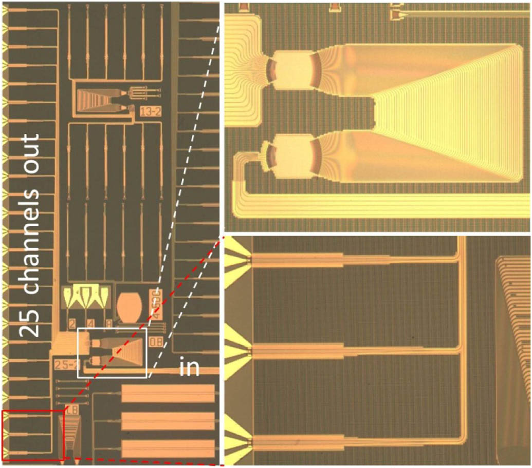
Figure 1.Top-view optical micrographs of the WDM receiver chip, AWG, and Ge-on-Si waveguide photodetector array.
3. RESULTS AND DISCUSSION
The current-voltage (I-V) characteristics and optical responsivity of standalone photodetectors were measured using the Agilent B1500A semiconductor parameter analyzer, a probe station, and a Santec tunable laser TSL-550 (1500–1630 nm) at room temperature. The incident light was coupled into the standalone photodetector from a grating coupler by a single-mode tapered fiber. To illustrate different optical coupling methods between the standalone photodetector and the WDM receiver chip, a schematic of the standalone photodetector coupling is shown in Fig. 2(a). The wavelength of the incident light is 1550 nm. The coupling loss between the tapered fiber and the grating coupler is about at 1550 nm. The optical power from the tapered fiber in the measurement is 0 dBm. Thus, the optical power entering the photodetector is about . Figure 2(a) presents the typical I-V curves of the standalone photodetector with/without light incidence from 1 to . The size of the Ge layer is . The I-V characteristics of the standalone photodetector exhibit good rectifying behavior. The on/off current ratio of the photodetector is higher than between 1 and , which can be attributed to the good quality of the Ge layer, p-i-n junction, and ohmic contact. The dark current of the photodetector is only 16.9 nA at , corresponding to the dark current density of . Due to the short length of the photodetector, the optical responsivity of the standalone photodetector at 1550 nm is 0.82 A/W at 0 V. The optical responsivity at 1550 nm does not change with the increase of reverse bias, which indicates that the strong built-in electric field induced by p-i-n junction is enough to extract photo-generated carriers. Spectral responsivity of the standalone photodetector from 1530 to 1580 nm under is shown in Fig. 2(b). The highest responsivity of 0.86 A/W is obtained at 1530 nm. Due to the decrease of absorption coefficient, the responsivity of the photodetector decreases gradually with the increasing of the wavelength. At 1580 nm, the responsivity is reduced to 0.37 A/W.

Figure 2.(a) Typical I-V curves of the standalone photodetector with/without light incidence (1550 nm) from 1 V to . The optical power entering the photodetector is about . The inset is a schematic of the optical coupling in this measurement. (b) Spectral responsivity of the standalone photodetector from 1530 to 1580 nm under .
The optoelectronic frequency responses of the standalone photodetectors are measured on the wafer by an Agilent light-wave component analyzer (LCA) N4373D with a 50 Ω-terminated GSG RF probe. The range of measured frequency is from 10 MHz to 40 GHz. The normalized frequency response of the photodetector at 1550 nm is presented in Fig. 3. Although the photodetector has a relatively large size (), it still exhibits a high bandwidth. The 3-dB bandwidth is as high as 23, 29, 31, and 32 GHz for the device at 0, , , and , respectively. The photodetector has a high bandwidth at zero bias, which also indicates the strong built-in electric field of the p-i-n junction.
Figure 3.Frequency response of a standalone photodetector at various reverse biases.
The photocurrent spectrum of the WDM receiver chip’s every channel is measured by different input optical wavelength from the tunable laser at room temperature. The incident light was coupled into the WDM receiver chip from the end face of the input waveguide by a single-mode tapered fiber. A schematic of this edge coupling is shown in Fig. 4(a). The coupling loss between the tapered fiber and the input waveguide is about . The optical power from the tapered fiber in this measurement is 0 dBm. Therefore, after removing input coupling loss between the input waveguide and tapered fiber, the optical power coupling into the input waveguide is about . The bias voltage of the integrated photodetectors is . Figure 4(a) shows the photocurrent spectra of the WDM receiver chip. The central wavelength is 1550.6 nm. The overall fiber-accessed responsivity of 0.09–0.24 A/W of the WDM receiver chip is directly calculated from the channels’ photocurrents (18–48 μA) and input optical power (). The photocurrent nonuniformity of the WDM receiver chip is about 4.1 dB, which is induced by the low responsivity of the photodetector at long wavelengths and the optical nonuniformity of the AWG. According to the responsivity of the standalone detector, the transmission through the AWG can be calculated from the photocurrent of each channel. Figure 4(b) shows the transmission spectra of the AWG. After removing the influence of the responsivity, the optical nonuniformity of the AWG is about 3.0 dB. The optical insertion loss of the AWG is about 5–8 dB. The optical insertion loss is attributed to the loss of bent waveguides, the sidewall roughness, the mode mismatch, and the loss difference between the center and marginal wavelength channels of the AWG. The largest optical insertion loss is found in channel 1, which has the longest waveguide among all the channels. The cross talk of the AWG is about . The average channel spacing is about 1.54 nm, which corresponds to 193 GHz. The performance of the AWG is in good agreement with our previous similar AWG without integrated photodetectors [13].
Figure 4.(a) Photocurrent spectrum of each channel of the WDM receiver chip. The inset is a schematic of the optical coupling in this measurement. (b) Transmission spectra of the 25-channel 200 GHz AWG.
Eye diagrams were measured on the wafer to study the high-speed receiving performance of the WDM receiver chip. The light with different wavelengths was coupled into a commercial modulator and was modulated into a long optical nonreturn-to-zero (NRZ) pseudorandom bit sequence data pattern at 40 and 50 Gbps by a bit pattern generator (SHF 12104A). The modulated light also was coupled into the WDM receiver chip from the end face of the input waveguide. The electrical signals from the different channels were displayed by a sampling oscilloscope (Keysight DCA-X 86100D) using an RF probe. A commercial RF amplifier (SHF 804M) with 23 dB gain was used to amplify the electrical signals. Eye diagrams of channels 5, 10, 15, 20, and 25 at 40 Gbps and 50 Gbps were obtained under a photocurrent of photodetector between 90 and 110 μA, as shown in Fig. 5. The modulator eye diagrams are also shown for comparison. The extinction ratios (ERs) of the 40 and 50 Gbps modulator eye diagrams are 7.4 and 6.5 dB, respectively. According to the responsivity of the standalone detector and the optical insertion loss of the AWG, the optical power coupling into the input waveguide of the WDM receiver chip can be calculated as , , , , and for these channels, corresponding to the net optical power into the photodetectors of , , , , and , respectively. These channels show clear open eye diagrams at 40 and 50 Gbps with such low optical power, even without reverse bias, which is an important characteristic to meet the low power consumption demands of a high-performance optical communication system. The difference among the eye diagrams of different channels is attributed to the difference of photocurrents, which can be clearly observed from the amplitude of these eye diagrams. Due to the deterioration of the modulator eye diagram and high sensitivity requirement of the photodetector at 50 Gbps, the 50 Gbps eye diagrams are not as good as the 40 Gbps eye diagrams. However, the 50 Gbps eye diagrams of the channels will become better as the input optical power increases. When the reverse bias is , the eye diagrams become a little wider than that at zero bias, which indicates the improvement of the bandwidth. When the reverse bias is larger than , the eye diagrams almost do not change further, which is in agreement with the bandwidth of the photodetector. The WDM receiver chip has 25 channels, and each channel can operate at 50 Gbps. Therefore, the total aggregate data receiving rate of this WDM receiver chip is 1.25 Tbps.
Figure 5.40 Gbps and 50 Gbps eye diagrams of channels 5, 10, 15, 20, and 25 at 0 and −1 V. The modulator eye diagrams are also shown for comparison.
The bit error rate (BER) of the receiver chip is roughly estimated from the factors of the eye diagrams under different input optical powers [16]. The BER curves of channel 10 at 40 and 50 Gbps are shown in Fig. 6. The wavelength of the input light is 1547.7 nm, which is the center wavelength of channel 10. The applied voltage of channel 10 is . Due to the limited optical power budget of our tunable laser, a higher optical power is not available. The BER sensitivity of channel 10 is predicted for input optical power of and 1.6 dBm at 40 and 50 Gbps, respectively. The 40 and 50 Gbps eye diagrams of channel 10 under and input optical power are also shown in Fig. 6. Due to higher input optical power, these eye diagrams are much better than those in Fig. 5. According to the 3.7 dB nonuniform responsivity among channels, the input optical power sensitivity (BER of ) of the WDM receiver chip is about and 1.6–5.3 dBm at 40 and 50 Gbps, respectively. Higher sensitivity would be realized by using a transimpedance amplifier (TIA) which has lower noise and higher gain than an RF amplifier. For comparison, performance of the reported Si photonic WDM receivers is shown in Table 1. Although the properties of our AWG are medium, due to the high performance of our photodetectors, especially at low bias voltage, our receiver chip exhibits much higher bit rate than other reported results.
| Demultiplexer | Platform | Insertion Loss (dB) | Cross Talk (dB) | Number of Channels | Receiving Bit Rate (Gbps) |
| Echelle grating [6] | 3 μm SOI | 2–4 | <−27 | 40 | 25 |
| Microring [8] | 220 nm SOI | 0.3 | <−20 | 8 | 20 |
| AMI [10] | 220 nm SOI | 0.5 | <−15 | 4 | 12.5 |
| AWG [11] | 300 nm SOI | 1.5–4.5 | <−18 | 32 | 10 |
| This work: AWG | 220 nm SOI | 5–8 | <−12 | 25 | 50 |
Table 1. Performance Comparison for Si Photonic WDM Receivers
Figure 6.BER curves of channel 10 at 40 and 50 Gbps. The 40 and 50 Gbps eye diagrams of channel 10 under and input optical power are shown for comparison.
4. SUMMARY
In summary, a high-performance WDM Si photonics receiver chip is fabricated and measured by monolithic integration of a 25-channel Si nanowire AWG with 200-GHz channel spacing and an array of high-speed waveguide Ge-on-Si photodetectors on the SOI platform. The optical insertion loss of the AWG is 5–8 dB, and its cross talk is . The dark current density, responsivity, and 3-dB bandwidth of the waveguide photodetector at are , 0.86–0.37 A/W at 1530–1580 nm, and 29 GHz, respectively. The responsivity of the WDM receiver chip is 0.09–0.24 A/W at , corresponding to the different channels. Every channel exhibits an open eye diagram at 50 Gbps with low input optical power even under zero bias. A 1.25 Tbps total aggregate data receiving rate of this WDM receiver chip is realized. The input optical power sensitivity (BER of ) of the WDM receiver chip is about and 1.6–5.3 dBm at 40 and 50 Gbps, respectively. This high-performance WDM Si photonics receiver chip constitutes a new milestone toward future high-speed data communication operating over 1 Tbps with low cost and low power.
References
[1] P. Dong. Silicon photonic integrated circuits for wavelength-division multiplexing applications. IEEE J. Sel. Top. Quantum Electron., 22, 370-378(2016).
[2] L. Chen, C. R. Doerr, L. Buhl, Y. Baeyens, R. A. Aroca. Monolithically integrated 40-wavelength demultiplexer and photodetector array on silicon. IEEE Photon. Technol. Lett., 23, 869-871(2011).
[3] M. Paniccia. Integrating silicon photonics. Nat. Photonics, 4, 498-499(2010).
[4] J. Michel, J. Liu, L. C. Kimerling. High-performance Ge-on-Si photodetectors. Nat. Photonics, 4, 527-534(2010).
[5] P. Dong, L. Chen, Y.-K. Chen. High-speed low-voltage single-drive push-pull silicon Mach-Zehnder modulators. Opt. Express, 20, 6163-6169(2012).
[6] D. Feng, W. Qian, H. Liang, B. J. Luff, M. Asghari. High-speed receiver technology on the SOI platform. IEEE J. Sel. Top. Quantum Electron., 19, 3800108(2013).
[7] H. Pan, S. Assefa, F. Horst, C. L. Schow, A. V. Rylyakov, W. M. J. Green, M. H. Khater, S. Kamlapurka, C. Reinholm, E. Kiewra, S. M. Shank, C. W. Baks, B. J. Offrein, Y. A. Vlasov. 250 Gbps 10-channel WDM silicon photonics receiver. 9th International Conference on Group IV Photonics (GFP), 162-164(2012).
[8] Q. Fang, Y. T. Phang, C. W. Tan, T.-Y. Liow, M. B. Yu, G. Q. Lo, D. L. Kwong. Multi-channel silicon photonic receiver based on ring-resonators. Opt. Express, 18, 13510-13515(2010).
[9] D. Y. Lee, X. Zheng, J. Yao, Y. Luo, J.-H. Lee, S. Lin, H. Thacker, J. Bovington, I. Shubin, S. S. Djordjevic, J. E. Cunningham, K. Raj, A. V. Krishnamoorthy. Error-free operation of a polarization-insensitive 4 × 25 Gbps silicon photonic WDM receiver with closed-loop thermal stabilization of Si microrings. Opt. Express, 24, 13204-13209(2016).
[10] C. G. Littlejohns, Y. Hu, F. Y. Gardes, D. J. Thomson, S. A. Reynolds, G. Z. Mashanovich, G. T. Reed. 50 Gb/s silicon photonics receiver with low insertion loss. IEEE Photon. Technol. Lett., 26, 714-717(2014).
[11] Q. Fang, T.-Y. Liow, J. F. Song, K. W. Ang, M. B. Yu, G. Q. Lo, D.-L. Kwong. WDM multi-channel silicon photonic receiver with 320 Gbps data transmission capability. Opt. Express, 18, 5106-5113(2010).
[12] S. Pathak, M. Vanslembrouck, P. Dumon, D. V. Thourhout, P. Verheyen, G. Lepage, P. Absil, W. Bogaerts. Effect of mask discretization on performance of silicon arrayed waveguide gratings. IEEE Photon. Technol. Lett., 26, 718-721(2014).
[13] P. Yuan, Y. Wang, Y. Wu, L. Liu, J. An, X. Hu. 25-channel 200 GHz AWG based on SOI ridge waveguides. J. Infrared Millim. Waves, 37, 692-697(2018).
[14] Z. Liu, F. Yang, W. Wu, H. Cong, J. Zheng, C. Li, C. Xue, B. Cheng, Q. Wang. 48 GHz high-performance Ge-on-SOI photodetector with zero-bias 40 Gbps grown by selective epitaxial growth. J. Lightwave Technol., 35, 5306-5310(2017).
[15] K. Li, J. Zhang, J. An, J. Li, L. Wang, Y. Wang, Y. Wu, X. Yin, X. Hu. Design and fabrication of 25-channel 200 GHz AWG based on Si nanowire waveguides. Optoelectron. Lett., 13, 241-244(2017).
[16] S. Ohteru, N. Takachio. Optical signal quality monitor using direct Q-factor measurement. IEEE Photon. Technol. Lett., 11, 1307-1309(1999).


