• Photonics Research
  • Vol. 7, Issue 6, B12 (2019)
Xianhe Liu1、2, Kishwar Mashooq1, David A. Laleyan1, Eric T. Reid1, and Zetian Mi1、*
Author Affiliations
  • 1Department of Electrical Engineering and Computer Science, University of Michigan, Ann Arbor, Michigan 48109, USA
  • 2Department of Electrical and Computer Engineering, McGill University, Montreal, Quebec H3A 0E9, Canada
  • show less
    DOI: 10.1364/PRJ.7.000B12 Cite this Article Set citation alerts
    Xianhe Liu, Kishwar Mashooq, David A. Laleyan, Eric T. Reid, Zetian Mi. AlGaN nanocrystals: building blocks for efficient ultraviolet optoelectronics[J]. Photonics Research, 2019, 7(6): B12 Copy Citation Text show less
    (a) Schematic of an AlGaN nanocrystal. (b) Top view of a photonic crystal structure. (c) Schematic for the scattering process in the photonic crystal structure. (d) Light-extraction efficiency (LEE) for the planar structure and the photonic crystal structure with a=160 nm and d=95 nm [61].
    Fig. 1. (a) Schematic of an AlGaN nanocrystal. (b) Top view of a photonic crystal structure. (c) Schematic for the scattering process in the photonic crystal structure. (d) Light-extraction efficiency (LEE) for the planar structure and the photonic crystal structure with a=160  nm and d=95  nm [61].
    (a) Photonic band structure of a photonic crystal with a lattice constant of 207 nm and a diameter of 144 nm. The inset is the top view showing the arrangement of nanocrystals. (b) The electric field distribution of the band-edge mode in the entire device.
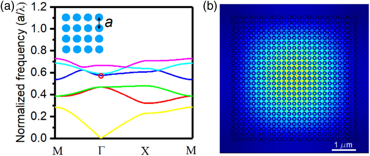
    Fig. 2. (a) Photonic band structure of a photonic crystal with a lattice constant of 207 nm and a diameter of 144 nm. The inset is the top view showing the arrangement of nanocrystals. (b) The electric field distribution of the band-edge mode in the entire device.
    Variation of (a) threshold current density and (b) linewidth at an injection current of 5×Ith with the device lateral dimension (L).
    Fig. 3. Variation of (a) threshold current density and (b) linewidth at an injection current of 5×Ith with the device lateral dimension (L).
    Far-field radiation pattern calculated for a photonic nanocrystal laser structure with a lattice constant of 207 nm and a diameter of 144 nm.
    Fig. 4. Far-field radiation pattern calculated for a photonic nanocrystal laser structure with a lattice constant of 207 nm and a diameter of 144 nm.
    (a) Schematic of the selective-area epitaxy process. (b) A typical SEM image of AlGaN nanocrystals grown by selective-area epitaxy. (c) Normalized PL spectra for AlGaN nanocrystals with Al content across nearly the entire compositional range [33].
    Fig. 5. (a) Schematic of the selective-area epitaxy process. (b) A typical SEM image of AlGaN nanocrystals grown by selective-area epitaxy. (c) Normalized PL spectra for AlGaN nanocrystals with Al content across nearly the entire compositional range [33].
    SEM images of (a) 0.5 μm GaN grown on Si wafer and (b) N-polar GaN nanocrystals grown on Si.
    Fig. 6. SEM images of (a) 0.5 μm GaN grown on Si wafer and (b) N-polar GaN nanocrystals grown on Si.
    (a) PL emission spectra of AlN and AlN:Mg nanostructures measured at room temperature. (b) Schematic illustration of the Mg impurity band of AlN nanostructures due to high Mg concentration and the reduced activation energy for a portion of Mg acceptors.
    Fig. 7. (a) PL emission spectra of AlN and AlN:Mg nanostructures measured at room temperature. (b) Schematic illustration of the Mg impurity band of AlN nanostructures due to high Mg concentration and the reduced activation energy for a portion of Mg acceptors.
    (a) I-V characteristics of a 300 μm×300 μm LED device at room temperature. Inset: schematic of the fabricated LED structure. (b) Room temperature EL spectra of the LED device for various injection currents [35].
    Fig. 8. (a) I-V characteristics of a 300  μm×300  μm LED device at room temperature. Inset: schematic of the fabricated LED structure. (b) Room temperature EL spectra of the LED device for various injection currents [35].
    (a) EL spectra of the Al tunnel junction AlGaN UV LED under CW biasing condition. Inset: EL spectrum in the logarithmic scale. (b) Variations of output power with injection current for Al tunnel junction AlGaN UV LED and standard p-i-n AlGaN UV LED. Inset: an optical image of the device under an injection current of 8 A/cm2 [31].
    Fig. 9. (a) EL spectra of the Al tunnel junction AlGaN UV LED under CW biasing condition. Inset: EL spectrum in the logarithmic scale. (b) Variations of output power with injection current for Al tunnel junction AlGaN UV LED and standard p-i-n AlGaN UV LED. Inset: an optical image of the device under an injection current of 8  A/cm2 [31].
    (a) Emission spectra for an AlGaN laser operating at 262 nm at 77 K under various injection current densities. (b) Variation of output with injection current. Blue circles represent the lasing peak. Black squares represent the background emission in the boxed area in (a) with a linewidth of 0.3 nm. The inset plots the data for the lasing peak in the logarithmic scale. Variations of (c) linewidth and (d) peak wavelength of the lasing peak at 262 nm with injection current density [30].
    Fig. 10. (a) Emission spectra for an AlGaN laser operating at 262 nm at 77 K under various injection current densities. (b) Variation of output with injection current. Blue circles represent the lasing peak. Black squares represent the background emission in the boxed area in (a) with a linewidth of 0.3 nm. The inset plots the data for the lasing peak in the logarithmic scale. Variations of (c) linewidth and (d) peak wavelength of the lasing peak at 262 nm with injection current density [30].
    (a) Emission spectra of an AlGaN laser device operating at 239 nm in CW biasing condition under different injection currents. (b) Variation of output with injection current for the lasing peak (red filled circles) and a non-lasing cavity mode (black open circles) from the boxed region in (a). The inset plots the data for the lasing peak in the logarithmic scale. (c) Variations of linewidth with the injection current [142].
    Fig. 11. (a) Emission spectra of an AlGaN laser device operating at 239 nm in CW biasing condition under different injection currents. (b) Variation of output with injection current for the lasing peak (red filled circles) and a non-lasing cavity mode (black open circles) from the boxed region in (a). The inset plots the data for the lasing peak in the logarithmic scale. (c) Variations of linewidth with the injection current [142].
    ParameterDefinition
    NCarrier concentration
    NphPhoton density in the cavity
    JCurrent density
    qElectron charge
    dTotal thickness of the active layers
    RrRadiative recombination rate
    RnrNonradiative recombination rate
    gMaterial gain
    cLight speed in vacuum
    nRefractive index of the active layers
    ΓoOptical confinement factor
    αTotal loss
    Table 1. Definition of Various Parameters Used in the Rate Equations
    Xianhe Liu, Kishwar Mashooq, David A. Laleyan, Eric T. Reid, Zetian Mi. AlGaN nanocrystals: building blocks for efficient ultraviolet optoelectronics[J]. Photonics Research, 2019, 7(6): B12
    Download Citation