• Photonics Research
  • Vol. 5, Issue 6, 649 (2017)
Tatiana Kovalevich1、*, Djaffar Belharet1, Laurent Robert1, Myun-Sik Kim2, Hans Peter Herzig2, Thierry Grosjean1, and Maria-Pilar Bernal1
Author Affiliations
  • 1Département d’Optique P. M. Duffieux, Institut FEMTO-ST, UMR 6174 CNRS, Université Bourgogne Franche-Comté, 15B Avenue des Montboucons, 25030 Besan?on Cedex, France
  • 2Optics & Photonics Technology Laboratory, Ecole Polytechnique Fédérale de Lausanne (EPFL), Rue de la Maladière 71b, Neuchatel CH-2000, Switzerland
  • show less
    DOI: 10.1364/PRJ.5.000649 Cite this Article Set citation alerts
    Tatiana Kovalevich, Djaffar Belharet, Laurent Robert, Myun-Sik Kim, Hans Peter Herzig, Thierry Grosjean, Maria-Pilar Bernal. Experimental evidence of Bloch surface waves on photonic crystals with thin-film LiNbO3 as a top layer[J]. Photonics Research, 2017, 5(6): 649 Copy Citation Text show less
    Thickness profile of the TFLN.
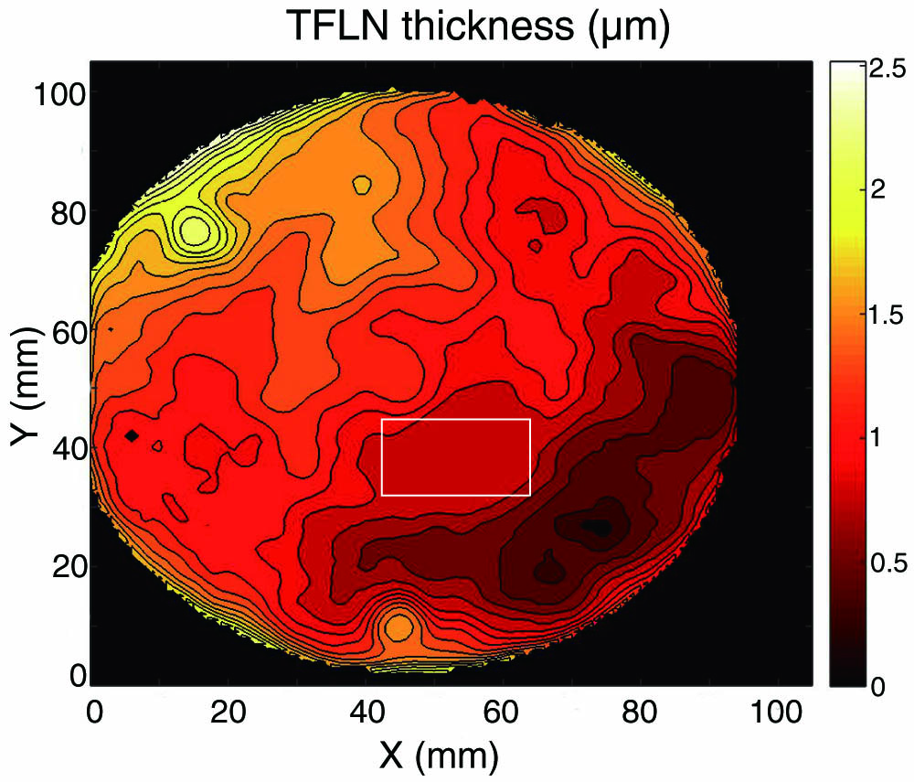
    Fig. 1. Thickness profile of the TFLN.
    Schematic of the membrane-based 1DPhC fabrication process: (a) bonding of bulk LiNbO3 to Si with Cr and Au, (b) LiNbO3 polishing, (c) photoresist deposition, (d) UV lithography of the photoresist, (e) DRIE etching of Si and wet etching of Cr and Au, (f) photoresist removal, and (g) multilayer deposition.
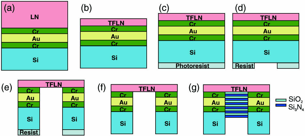
    Fig. 2. Schematic of the membrane-based 1DPhC fabrication process: (a) bonding of bulk LiNbO3 to Si with Cr and Au, (b) LiNbO3 polishing, (c) photoresist deposition, (d) UV lithography of the photoresist, (e) DRIE etching of Si and wet etching of Cr and Au, (f) photoresist removal, and (g) multilayer deposition.
    (a) Microscope images of the membranes. (b) Microscope images of the membranes after multilayer deposition.
    Fig. 3. (a) Microscope images of the membranes. (b) Microscope images of the membranes after multilayer deposition.
    (a) FIB-SEM image of the membrane. (b) FIB-SEM image of the 1DPhC (suspended membrane).
    Fig. 4. (a) FIB-SEM image of the membrane. (b) FIB-SEM image of the 1DPhC (suspended membrane).
    Schematic of the on-glass 1DPhC fabrication process: (a) obtaining TFLN with smart cut technology, (b) multilayer deposition, (c) UV glue bonding to the glass substrate, (d) protection of the sample with photoresist, (e) DRIE etching of Si and RIE etching of SiO2, and (f) photoresist removal.
    Fig. 5. Schematic of the on-glass 1DPhC fabrication process: (a) obtaining TFLN with smart cut technology, (b) multilayer deposition, (c) UV glue bonding to the glass substrate, (d) protection of the sample with photoresist, (e) DRIE etching of Si and RIE etching of SiO2, and (f) photoresist removal.
    (a) Dispersion curves for the on-membrane 1DPhC. (b) Dispersion curves for the on-glass 1DPhC.
    Fig. 6. (a) Dispersion curves for the on-membrane 1DPhC. (b) Dispersion curves for the on-glass 1DPhC.
    (a) Experimental setup for the on-membrane 1DPhC. (b) Experimental setup for the on-glass 1DPhC.
    Fig. 7. (a) Experimental setup for the on-membrane 1DPhC. (b) Experimental setup for the on-glass 1DPhC.
    (a) Camera image intensity profile of the BWS-related reflectance dip for the membrane-based sample. (b) Camera image intensity profile of the BWS-related reflectance dip for the on-glass sample.
    Fig. 8. (a) Camera image intensity profile of the BWS-related reflectance dip for the membrane-based sample. (b) Camera image intensity profile of the BWS-related reflectance dip for the on-glass sample.
    Tatiana Kovalevich, Djaffar Belharet, Laurent Robert, Myun-Sik Kim, Hans Peter Herzig, Thierry Grosjean, Maria-Pilar Bernal. Experimental evidence of Bloch surface waves on photonic crystals with thin-film LiNbO3 as a top layer[J]. Photonics Research, 2017, 5(6): 649
    Download Citation