Abstract
Strong nonlinear, electro-optical, and thermo-optical properties of lithium niobate (LN) have gained much attention. However, the implementation of LiNbO3 in real devices is not a trivial task due to difficulties in manufacturing and handling thin-film LN. In this study, we investigate an optical device where the Bloch surface wave (BSW) propagates on the thin-film LN to unlock its properties. First, access to the LN film from air (or open space) is important to exploit its properties. Second, for sustaining the BSW, one-dimensional photonic crystal (1DPhC) is necessary to be fabricated under the thin-film LN. We consider two material platforms to realize such a device: bulk LN and commercial thin-film LN. Clear reflectance dips observed in far-field measurements demonstrate the propagation of BSWs on top of the LN surface of the designed 1DPhCs.1. INTRODUCTION
Lithium niobate (LN) is a high refractive index birefringent crystal with tunable optical properties. It is widely used for integrated optics due to its excellent ferroelectrical, piezoelectrical, and thermoelectrical properties, its transparency over a wide wavelength range (350–5200 nm), its nonlinear optical polarizability, and its Pockels effect [1]. In order to improve the performance of integrated optical devices, several research groups have developed different structures, such as ridge waveguides, photonic crystal waveguides, and periodically poled lithium niobate structures [2]. As a high refractive index material, LN as a top layer is used for enhanced light confinement for many devices [3] and thin-film (TFLN) should be used to improve the confinement even more.
In this work, we propose two different novel architectures that can generate Bloch surface waves (BSWs) at TFLN layers. BSWs perform a strong field confinement at the interface between a periodic dielectric multilayer and a surrounding medium due to Bragg reflection and total internal reflection on two sides of the interface, respectively [4]. Light coupling can be easily achieved by a grating coupler [5] or by using the Kretschmann configuration [6,7]. Both coupling methods are simpler and more efficient in terms of coupling losses than the fiber-to-fiber coupling technique that is employed to horizontally excite a guided mode on TFLN [8].
Moreover, BSWs can be considered as an attractive alternative to surface plasmon polaritons due to the low loss features of dielectric materials in comparison with metals [6,9]. Therefore, these dielectric surface modes dramatically increase the light propagation length [7]. They were initially proposed for vapor sensing [10], biosensing [6], fluorescence studies [11], and for integrated optics [9,12]. The development of BSW-based devices has also profited a great deal from the development of different deposition techniques, such as atomic layer deposition [13,14] or plasma-enhanced chemical vapor deposition (PECVD) [15]. These techniques have allowed us to achieve the necessary precision in the manufacturing of subwavelength thickness layers required for the fabrication of BSW devices. Various materials constituting multilayer structures have been used in different designs of one-dimensional photonic crystal (1DPhC), offering a large panel of configurations for different applications at different wavelengths. The BSW propagation can be controlled by manipulating the refractive index inside the device [12].
Sign up for Photonics Research TOC. Get the latest issue of Photonics Research delivered right to you!Sign up now
In this work, we propose a 1DPhC with a TFLN as the top layer of the multilayer structure. The bonding into the 1DPhC structure brings anisotropy into the whole crystal, allowing the tunability of the BSW devices [16]. In previously studied 1DPhC with TFLN, the BSW is excited at the interface, where is an external medium. In that geometry, the BSW propagates on the surface of the TFLN, which is embedded within the multilayer. This geometry limits the use of such a device and cannot, for instance, be applied for sensing applications, where the evanescent tail of the BSW needs to be in the contact with the external environment to be sensed.
Direct electric field or temperature application cannot introduce a shift of the refractive index significant enough to shift the dispersion curve of 1DPhC directly. However, the refractive index change of up to is routinely produced by additional nanostructuring of [17]. Photonics crystals and Bragg gratings are some of the optical functions that can enhance the electro- and thermo-optical properties of -based devices. To do so in the BSW platform, access to from the top of 1DPhC is required.
Additionally, nonlinear properties of BSWs are attractive topics for study. Recently, phase-matched third-harmonic generation via doubly resonant optical surface modes [18] was achieved on the base of 1DPhC coated with a 15 nm GaAs film. Unfortunately, GaAs is not transparent in the visible range of wavelengths and is not suitable for many optical applications. The use of would be a perfect solution for future studies of BSW-induced nonlinearities on the TFLN surface. Once again to unlock the nonlinear properties of BSWs on , it is necessary to have an interface between and air [19].
2. FABRICATION, EXPERIMENTAL DETAILS, AND DISCUSSION
We present a BSW-based device, which is able to sustain surface waves at the interface. Two different geometries have been studied, fabricated, and optically characterized. The first one is based on the membrane, and the second one is held by a stable glass platform.
As we have mentioned before, the 1DPhC that sustain surface waves requires subwavelength thickness layers. In the case of LN, this requirement is challenging, especially because it needs to maintain its crystallinity in order to use the nonlinear properties of the material. Current technologies, such as sputtering, evaporation, or epitaxial growth of , only allow amorphous or polycrystalline films [20].
In order to achieve the desired LN properties and to avoid light scattering on the multilayer top surface a single-crystal TFLN bonded to an layer on an Si substrate [21] has been used for the on-glass 1DPhC as a first configuration.
A second configuration has been also fabricated using a single-crystal TFLN bonded to a Cr and Au layer on an Si substrate [22], which is thereafter bonded to the 1DPhC. For this geometry, the multilayer used was composed of Si/Au/Cr/Au/TFLN. The layer’s thicknesses were 500 μm for Si, 20 nm for both layers of Cr, 400 nm for the Au layer, and about 2 μm for the TFLN, respectively. In this case, the TFLN was manufactured by polishing of bulk bonded to an Si wafer by Au and Cr [22]. The thickness profile of the TFLN is shown in Fig. 1. For the manufacturing of 1DPhC, an LN sample with a thickness of 1.1 μm was used.
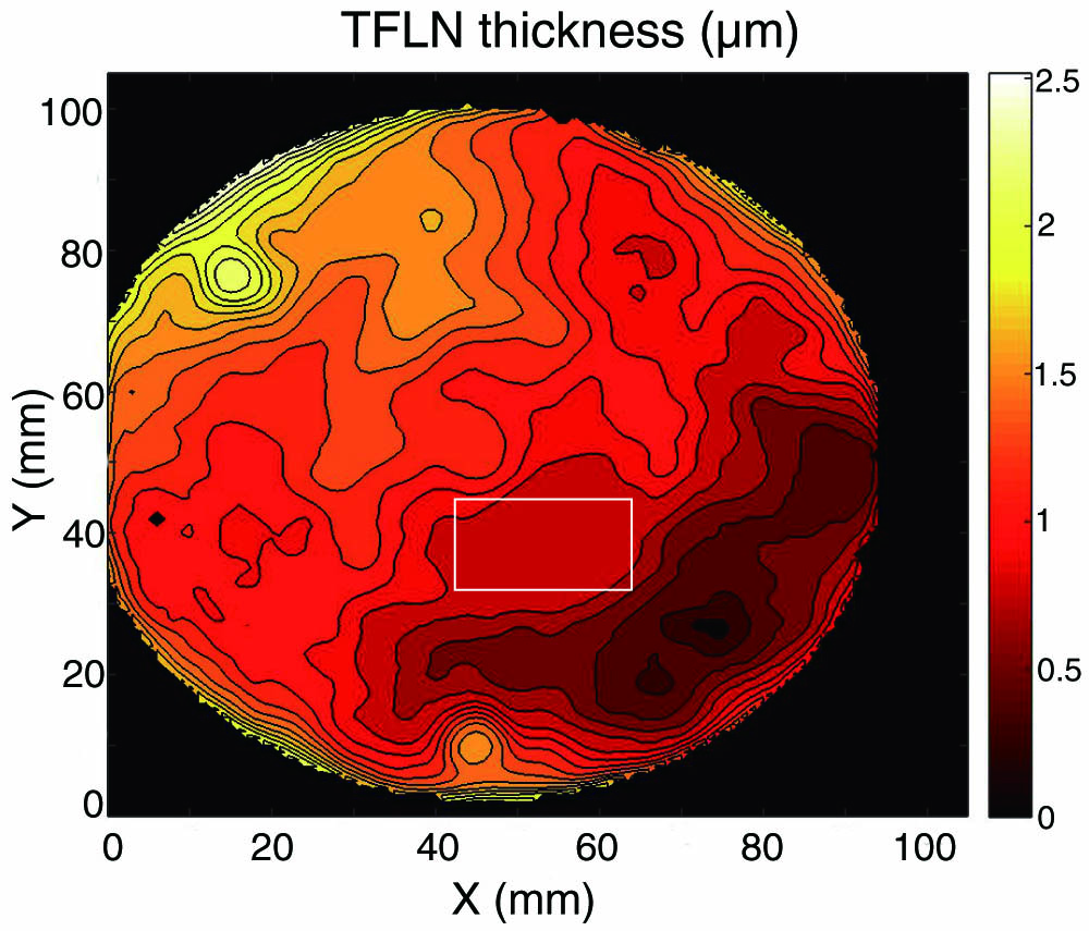
Figure 1.Thickness profile of the TFLN.
The 1DPhC was manufactured according to the steps shown in Fig. 2. After the thinning of , a positive photoresist AZ 9260 was used for UV lithography.

Figure 2.Schematic of the membrane-based 1DPhC fabrication process: (a) bonding of bulk to Si with Cr and Au, (b) polishing, (c) photoresist deposition, (d) UV lithography of the photoresist, (e) DRIE etching of Si and wet etching of Cr and Au, (f) photoresist removal, and (g) multilayer deposition.
500 μm of an Si layer was removed by deep reactive ion etching (DRIE) [23] on SPTS equipment tooled by a dual plasma source (Rapier). Concerning the plasma etching process, a Bosch process with three sequences (Teflon deposition, Teflon removal in the trench bottom, and silicon etching) was used [24]. These three sequences were repeated in order to have an anisotropic wall’s profile (close to 90°); the Teflon deposition was performed by gas, and the etching sequence was achieved by using gas. The etch rate was 11 μm/min, and the selectivity was 1:180, which is the ratio between the AZ 9260 photoresist etch rate to the silicon etching rate.
Cr and Au were removed by a standard chemical wet etching process in Cr and Au etching solutions.
Concerning the multilayer fabrication, six periods of and were alternately deposited on top of the TFLN membrane suspended in air by PECVD (PlasmaLab 80 Plus by Oxford). The precursor gases for the deposition were , , and , and the process temperature was 300°C.
Membranes of two different areas were manufactured: and . The microscope images of the membranes are shown in Fig. 3(a). After the deposition of the multilayers, the membranes undergo some stretching, which is clearly seen from Fig. 3(b). This effect is stronger for the bigger membrane. The curvature of the membrane leads to the change of the incident angle for the BSW excitation, inducing uncertainties in the BSW propagation.
Figure 3.(a) Microscope images of the membranes. (b) Microscope images of the membranes after multilayer deposition.
Focused ion beam scanning electron microscope (FIB-SEM) images (Fig. 4) show the thicknesses of the layers. The thickness of was about 215 nm and of about 200 nm. The top layer of Cr seen in Fig. 4(b) was deposited in order to avoid charge effects during the measurements and was removed by the wet etching process.
Figure 4.(a) FIB-SEM image of the membrane. (b) FIB-SEM image of the 1DPhC (suspended membrane).
The manufacturing steps for the on-glass 1DPhC are shown in Fig. 5. In this case, single-crystal -cut TFLN of 400 nm bonded to an layer on an LN substrate [21] has been used. The TFLN was prepared using the He+ ion implantation technique. As in the previous sample, the multilayer stack of alternating and were deposited on TFLN by PECVD. The whole structure was bonded to the glass holder (500 μm) by UV glue. The UV glue (VITRALIT 6127) was chosen in such a way that its refractive index is close to the refractive index of glass. The top Si layer of Si was thinned down by polishing from 400 to 20 μm.
Figure 5.Schematic of the on-glass 1DPhC fabrication process: (a) obtaining TFLN with smart cut technology, (b) multilayer deposition, (c) UV glue bonding to the glass substrate, (d) protection of the sample with photoresist, (e) DRIE etching of Si and RIE etching of , and (f) photoresist removal.
The whole stack was protected by S1813 photoresist, and the 20 μm of Si was dry etched by DRIE. For this etching, the Bosch process was also employed. A 2 μm thickness layer of was etched by reactive ion etching (RIE) with a mixture of fluorine gases (—10 sccm and —5 sccm). After Si and etching, the remaining photoresist was chemically removed by using an acetone bath, followed by an ethanol bath, and finally by DI water. After inspection on the optical microscope, some photoresist residuals were still present. plasma (power 600 W, ) over 15 min was used to remove them.
After the manufacturing we obtained two different LN BSW-based devices. The multilayer of the membrane-based crystal was as follows: air/six pairs of (200 nm) and (215 nm)/TFLN(1.1 μm)/air.
The multilayer of the glass-supported crystal was as follows: glass/UV glue/six pairs of (220 nm) and (490 nm)/TFLN(386 nm)/air. In the green part of the spectrum (Fig. 6), one can observe a bandgap corresponding to the multilayer. Dispersion curves are shown in Fig. 6 for both samples. At the wavelength of 473 nm, refractive indices of multilayer compounds are , , , and . In order to obtain the dispersion curves, a standard impedance approach was used [25]. In the case of the membrane sample, light can be coupled into the BSW at the incident angle of 59° and at 56° for the glass-supported sample, as shown in Fig. 6.
Figure 6.(a) Dispersion curves for the on-membrane 1DPhC. (b) Dispersion curves for the on-glass 1DPhC.
In order to achieve experimental values for and to confirm them with the theoretical predictions, the Kretschmann configuration was used for light coupling (Fig. 7). TE-polarized light from a diode laser (Spectra-Physics Excelsior) was focused on the sample (). A BK7 prism was fixed on a rotational stage, which allowed us to change the incidence angle until the obtention of BSW excitation. Refractive index matching oil was used for both samples as a connecting media between the sample and the prism. Reflected light was detected with a CCD camera (mV BlueFox 120GU). The BSW absorption lines were detected at 61° for the membrane and 55° for the glass-supported sample. We can therefore observe that the experimentally achieved angles are slightly different from the theoretical ones. This shift may be due to the difference of requested and experimentally achieved thicknesses of the multilayers as well as due to some inaccuracies of refractive index values.
Figure 7.(a) Experimental setup for the on-membrane 1DPhC. (b) Experimental setup for the on-glass 1DPhC.
The images of the reflected light at the angle of BSW excitation were collected. In Fig. 8, the normalized intensity along the image profile at the dip area is shown for both samples. In the case of the membrane, the dip is narrower and the reflectance dumps for 60%. For the glass-supported sample, the dip is 1.3 times wider and only 40% of reflectance dumping is observed. The bigger dumping of reflectance for the membrane sample indicates that in this case we have better coupling of light into the BSW than for the on-glass 1DPhC. However, in the case of the membrane, significant aberrations due to the curvature of the membrane occur.
Figure 8.(a) Camera image intensity profile of the BWS-related reflectance dip for the membrane-based sample. (b) Camera image intensity profile of the BWS-related reflectance dip for the on-glass sample.
We can therefore conclude that the multilayer on the glass support is more stable and provides a bigger area for light manipulation that uses the BSW (in our case area). This advantage can be used for BSW-based on-chip integrated optics [26]. However, additional manipulations (such as polishing, plasma etching of Si and , as well as photoresist removal) introduce some deformations into the layer structure. This leads to a decrease in the coupling efficiency and propagation length of BSW, which can be observed from the broadening of the BSW-related absorption dip.
In the case of the membrane configuration, we have limited access to the multilayer for the BSW coupling on the Kretschmann configuration (in our case, a maximum area is available). This limitation can be overcome, for example, by using a grating coupler [5]. In addition, the whole membrane with the multilayer can be transferred and bonded into a fiber tip. This fibered configuration can be used for BSW-based lab-on-fiber systems with TFLN as a part of it. For the membrane multilayer, a strong BSW coupling was observed [as shown in Fig. 8(a)], though there are still additional perturbations for the light propagation, which are due to the membrane curvature.
In this work, we show theoretically and experimentally the excitation of BSWs at a TFLN/air interface, which introduces all the potentialities of the functionalities through BSW light guiding.
3. CONCLUSIONS
We have demonstrated BSWs on top of TFLN in two different configurations. LN-based photonic crystals, which are able to sustain BSWs, were designed and fabricated at the base of a TFLN membrane and on a glass support. In order to compare two different 1DPhCs, far-field measurements were done. The designed 1DPhCs allowed us to obtain BSWs at the TFLN/air interface for TE-polarized light at a wavelength of 473 nm. Such designs of the 1DPhCs, together with the use of the nonlinear properties of , open up the possibility of creating BSW-based active tunable devices.
Acknowledgment
Acknowledgment. The authors thank the NANOLN company for providing thin-film LiNbO3 samples.
References
[1] J. E. Toney. Lithium Niobate Photonics(2015).
[2] W. Sohler, H. Hu, R. Ricken, V. Quiring, C. Vannahme, H. Herrmann, H. Suche. Integrated optical devices in lithium niobate. Opt. Photon. News, 19, 24-31(2008).
[3] A. Guarino, G. Poberaj, D. Rezzonico, R. Degl’Innocenti, R. P. Gunter. Electro-optically tunable microring resonators in lithium niobate. Nat. Photonics, 1, 407-410(2007).
[4] P. Yeh, A. Yariv, L. Sun, C. S. Hong. Electromagnetic propagation in periodic stratified media. I. General theory. J. Opt. Soc. Am., 67, 423-438(1977).
[5] T. Kovalevich, P. Boyer, M. Suarez, R. Salut, M.-S. Kim, H. P. Herzig, M. P. Bernal. Polarization controlled directional propagation of Bloch surface wave. Opt. Express, 25, 5710-5715(2017).
[6] V. N. Konopsky, E. V. Alieva. Photonic crystal surface waves for optical biosensors. Anal. Chem., 79, 4729-4735(2007).
[7] R. Dubey, E. Barakat, M. Häyrinen, M. Roussey, S. Honkanen, M. Kuittinen, H. P. Herzig. Experimental investigation of the propagation properties of Bloch surface waves on dielectric multilayer platform. J. Eur. Opt. Soc., 13, 5(2017).
[8] A. Gerthoffer, C. Guyot, W. Qiu, A. Ndao, M. P. Bernal, N. Courjal. Strong reduction of propagation losses in LiNbO3 ridge waveguides. Opt. Mater., 38, 37-41(2014).
[9] E. Descrovi, T. Sfez, M. Quaglio, D. Brunazzo, L. Dominici, F. Michelotti, H. P. Herzig, O. Martin, F. Giorgis. Guided Bloch surface waves on ultrathin polymeric ridges. Nano Lett., 10, 2087-2091(2010).
[10] F. Michelotti, B. Sciacca, L. Dominici, M. Quaglio, E. Descrovi, F. Giorgis, F. Geobaldo. Fast optical vapour sensing by Bloch surface waves on porous silicon membranes. Phys. Chem. Chem. Phys., 12, 502-506(2010).
[11] A. Sinibaldi, A. Fieramosca, R. Rizzo, A. Anopchenko, N. Danz, P. Munzert, C. Magistris, C. Barolo, F. Michelotti. Combining label-free and fluorescence operation of Bloch surface wave optical sensors. Opt. Lett., 39, 2947-2950(2014).
[12] L. Yu, B. Barakat, T. Sfez, L. Hvozdara, J. Di Francesco, H. P. Herzig. Manipulating Bloch surface waves in 2D: a platform concept-based flat lens. Light Sci. Appl., 3, e124(2014).
[13] R. L. Puurunen. A short history of atomic layer deposition: Tuomo Suntola’s atomic layer epitaxy. Chem. Vap. Deposition, 20, 332-344(2014).
[14] N. Häyrinen, J. Leon Shohet, M. Roussey, A. Bera, M. Kuittinen, S. Honkanen. Atomic layer re-deposition for nanoscale devices. Encyclopedia of Plasma Technology(2015).
[15] G. Lucovsky, D. V. Tsu. Plasma enhanced chemical vapor deposition: differences between direct and remote plasma excitation. J. Vac. Sci. Technol. A, 5, 2231-2238(1987).
[16] T. Kovalevich, A. Ndao, M. Suarez, M. Häyrinen, M. Roussey, M. Kuittinen, T. Grosjean, M. P. Bernal. Tunable Bloch surface waves in anisotropic photonic crystals based on lithium niobate thin films. Opt. Lett., 41, 5616-5619(2016).
[17] M. Roussey, M. P. Bernal, N. Courjal, D. Van Labeke, F. I. Baida, R. Salut. Electro-optic effect exaltation on lithium niobate photonic crystals due to slow photons. Appl. Phys. Lett., 89, 241110(2006).
[18] V. N. Konopsky, E. V. Alieva, S. T. Alyatkin, A. A. Melnikov, S. V. Chekalin, V. M. Agranovich. Phase-matched third-harmonic generation via doubly resonant optical surface modes in 1D photonic crystals. Light Sci. Appl., 5, e16168(2016).
[19] A. D. Bezpaly, V. M. Shandarov. Optical formation of waveguide elements in photorefractive surface layer of a lithium niobate sample. Phys. Procedia, 86, 166-169(2017).
[20] V. Joshkin, K. Dovidenko, S. Oktyabrsky, D. Saulys, T. Kuech, L. McCaughan. New methods for fabricating patterned lithium niobate for photonic applications. J. Cryst. Growth, 259, 273-278(2003).
[21] H. Han, L. Cai, H. Hu. Optical and structural properties of single-crystal lithium niobate thin film. Opt. Mater., 42, 47-51(2015).
[22] F. Bassignot, E. Courjon, S. Ballandras, J. M. Lesage, R. Petit. Acoustic resonator based on periodically poled transducers: fabrication and characterization. J. Appl. Phys., 112, 074108(2012).
[23] C. B. Labelle, V. M. Donnelly, G. R. Bogart, R. L. Opila, A. Kornblit. Investigation of fluorocarbon plasma deposition from cC4F8 for use as passivation during deep silicon etching. J. Vac. Sci. Technol. A, 22, 2500-2507(2004).
[24] F. Laermer, A. Schilp. Method of anisotropically etching silicon. U.S. patent(1996).
[25] V. N. Konopsky. Plasmon-polariton waves in nanofilms on one-dimensional photonic crystal surfaces. New J. Phys., 12, 093006(2010).
[26] R. Dubey, B. Vosoughi Lahijani, E. Barakat, M. Häyrinen, M. Roussey, M. Kuittinen, H. P. Herzig. Near-field characterization of a Bloch-surface-wave-based 2D disk resonator. Opt. Lett., 41, 4867-4870(2016).


