Abstract
Planar semiconductor InGaAs/InP single photon avalanche diodes with high responsivity and low dark count rate are preferred single photon detectors in near-infrared communication. However, even with well-designed structures and well-controlled operational conditions, the performance of InGaAs/InP SPADs is limited by the inherent characteristics of avalanche process and the growth quality of InGaAs/InP materials. It is difficult to ensure high detection efficiency while the dark count rate is controlled within a certain range at present. In this paper, we fabricated a device with a thick InGaAs absorption region and an anti-reflection layer. The quantum efficiency of this device reaches 83.2%. We characterized the single-photon performance of the device by a quenching circuit consisting of parallel-balanced InGaAs/InP single photon detectors and single-period sinusoidal pulse gating. The spike pulse caused by the capacitance effect of the device is eliminated by using the characteristics of parallel balanced common mode signal elimination, and the detection of small avalanche pulse amplitude signal is realized. The maximum detection efficiency is 55.4% with a dark count rate of 43.8 kHz and a noise equivalent power of 6.96 × 10?17 W/Hz1/2 at 247 K. Compared with other reported detectors, this SPAD exhibits higher SPDE and lower noise-equivalent power at a higher cooling temperature.Planar semiconductor InGaAs/InP single photon avalanche diodes with high responsivity and low dark count rate are preferred single photon detectors in near-infrared communication. However, even with well-designed structures and well-controlled operational conditions, the performance of InGaAs/InP SPADs is limited by the inherent characteristics of avalanche process and the growth quality of InGaAs/InP materials. It is difficult to ensure high detection efficiency while the dark count rate is controlled within a certain range at present. In this paper, we fabricated a device with a thick InGaAs absorption region and an anti-reflection layer. The quantum efficiency of this device reaches 83.2%. We characterized the single-photon performance of the device by a quenching circuit consisting of parallel-balanced InGaAs/InP single photon detectors and single-period sinusoidal pulse gating. The spike pulse caused by the capacitance effect of the device is eliminated by using the characteristics of parallel balanced common mode signal elimination, and the detection of small avalanche pulse amplitude signal is realized. The maximum detection efficiency is 55.4% with a dark count rate of 43.8 kHz and a noise equivalent power of 6.96 × 10?17 W/Hz1/2 at 247 K. Compared with other reported detectors, this SPAD exhibits higher SPDE and lower noise-equivalent power at a higher cooling temperature.Introduction
Semiconductor avalanche single photon detectors have great potential in engineering applications due to their low cost, small size and no need for ultra-low temperature, such as high-resolution spectroscopic measurements[1], quantum key distribution[2,3], non-destructive testing (NDT)[4], biological imaging[5], eye-safe laser ranging (LIDAR)[6], extreme imaging scenarios[7], optical time-domain reflectometry (OTDR)[8], and so on. These applications require SPAD to have high photon detection efficiency (PDE), low dark count rate (DCR) and low noise equivalent power (NEP). To determine a quantum state or distinguish a quantum bit in practical applications, SPAD usually works in Geiger mode.
As the core parameters to describe the performance of SPAD, high detection efficiency and low dark count are the main goals pursued by SPAD research, which mainly focus on improving materials quality, optimizing the device structure of the SPAD, reducing the operating temperature, improving the peripheral control driving technology of single photon detectors, and so on. For example, the well-developed SAGCM structure has achieved good results in reducing the dark current of the device[9]. In improving the peripheral control driving technology of single photon detector, many approaches have been reported, such as two matched delay lines[10], a capacitance balance method that matches the value of SPAD capacitance[11,12], self-differential method[13,14], dual SPAD biased in parallel with differential detection[15-19], sine gating method[20,21] and so on.
However, the performance of InGaAs/InP SPAD is still limited by the low growth quality of InGaAs/InP materials and the uncertainty of avalanche process, even with well-designed structure and excellent signal-to-noise ratio peripheral test circuits. It is difficult to ensure high detection efficiency while the dark count rate is controlled within a certain range at present. Since the high dark count rate greatly degrades the performance of InGaAs/InP SPADs, extensive research[22-25] has been undertaken to reduce the dark count rate by improving the material growth quality of InGaAs/InP SPADs, developing better and easier-to-control device fabrication techniques, and optimizing the device operating conditions.
Furthermore, the single-photon detection efficiency (PDE) of conventional InGaAs/InP SPADs depends on both avalanche probability and external quantum efficiency. Even with optimized structures, such as thick InGaAs absorber layer[26], back-incidence with the reflection layer[27], DBR-metal reflector[28], a selective area growth (SAG) method[29], InGaAs/InP SPAD could have very good external quantum up to 90% or higher in both communication bands of 1550 nm and 1310 nm effectiveness. The avalanche probability (AP) is inherently limited by the probability distribution of the gain in the collision ionization process. The gain of avalanche triggered by a single carrier has a very wide probability distribution, but high gain events that are favorable for detectable signals occur only in a fraction of the probability distribution. At the same time, the avalanche probability caused by multiple dark carriers is concentrated in a large gain range, which leads to the fact that the dark count probability rises faster with the electric field than that the probability of a single photon triggering a detectable signal in the multiplication region. This makes it difficult to obtain a single photon detector with more than 50% PDE and a reasonable low DCR[30].
In this paper, we fabricated a 20-µm-diameter APD with a thick (2.2µm) InGaAs absorption layer and an anti-reflection layer to improve its external quantum efficiency. At room temperature, the bulk dark current of the APD associated with dark counts was 23 pA, and at 1550 nm, the device external quantum efficiency is larger than 80%. The single-photon performance of the device was characterized by using a quenching circuit consisting of parallel-balanced InGaAs/InP single photon avalanche diodes and single-period sinusoidal pulse gating. The parallel balanced 20-µm-diameter InGaAs/InP single photon avalanche diodes operated in a single period sinusoidal pulse gated mode with a data transmission rate of up to 1 MHz, its maximum detection efficiency is 55.4% with a DCR of 43.8 kHz and a NEP of 6.96 × 10⁻¹⁷ W/Hz1/2 at 247 K . Compared with other reported detectors, this SPAD exhibits higher SPDE and lower noise-equivalent power at higher temperature.
Device fabrication
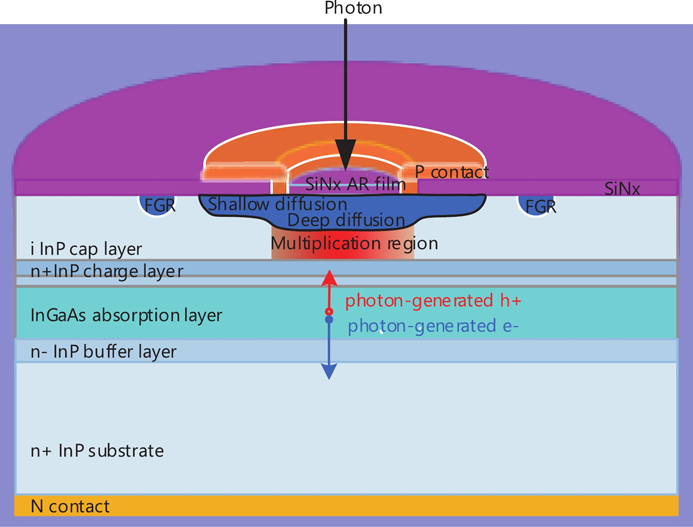
In this paper, we fabricated a single photon avalanche diode (SPAD) with separate absorption, grading, charge, and multiplication (SAGCM) structure,the structure of SAPD is shown inFig. 1. The device is a front illuminated planar In0.53Ga0.47As/InP APD with a diameter of 20µm, and it is grown by metalorganic chemical vapor disposition (MOCVD). The chip structure of the device has an N-type InP buffer layer on an N-type InP substrate, a 2.2μm intrinsic InGaAs absorption layer, three intrinsic InGaAsP grading layers with a thickness of 40 nm, an N-type InP charge layer with a thickness of 200 nm, and a 3.5μm intrinsic InP cap layer[31]. In the intrinsic InP cap layer, a shallow and deep diffusion of Zinc form a double p-type heavily doped diffusion. The double Zn diffusion is generated by two processes. The former diffusion forms a shallow central junction and a floating guard ring (FGR), and the latter diffusion forms the deep central junction which controls the thickness of the multiplier layer to 1.0μm and the diameter of the active area to 20μm. The diffusion step formed after these two diffusion processes is 400 nm. A layer of 215 nm SiNx AR film optimized for 1550 nm is deposited on the surface. The anode metal (Ti/Pt/Au) is sputtered on a part of the deep diffusion region at the top of APD and made the ringlike electrode, which makes the actual photosensitive diameter to 16μm.

Figure 1.(Color online) Structure Diagram of the SPAD.
Aiming to reduce SPAD dark count rate without lowering PDE, it is essential to optimize the vertical layer structure of the detector and its diffusion profile. Therefore, we adjusted the order of the double Zinc diffusion in the SPAD diffusion process. The first step is to diffuse the central shallow diffusion junction and the guard ring, and the second step is to diffuse the central deep diffusion junction based on the central shallow diffusion with the diffusion step of 400 nm. As shown inFig. 2(a), such a diffusion sequence finally forms a diffusion pattern with a gentle transition from the edge of the central deep diffusion region to the shallow diffusion region, so that the edge breakdown effect of the device can be well suppressed,Fig. 2(b) shows the simulated electric field distribution along the red dot line inFig. 2(a) when the reverse excess bias voltage (Vex) is 0.5 V above breakdown voltage. We found that the relative position of the maximum electric field shifted to the center as the device diffusion window size decreased by simulation and experiment. For smaller size devices, the vertical position of the maximum electric field coincided with the path of incident photons entering the device, which consequently increases the avalanche breakdown probability of photo-generated carriers that generated in the absorber and injected into the high field region when the diode is biased above breakdown, thereby improving the detection efficiency of the device. At the same time, due to the concentrated distribution of the high electric field strength of the device, the average breakdown probability of bulk dark carriers generated in the SPAD is reduced, so as to improve the overall signal-to-noise performance of the device. The diffusion profile characteristics of the diffusion mentioned in this paper and a quantitative analysis of the edge breakdown effect under different diffusion window sizes have been described in details in our published paper[31].
Figure 2.(Color online) (a) Edge of double diffusion profile of the optimized device observed by SEM. (b) Simulated optimized device electric field diagram after breakdown (Vex = 0.5 V).
Performance
Linear mode performance characteristic
Fig. 3(a) shows the typical dark current versus bias voltage (I–V) of a 20µm diameter SPAD at temperatures from 235 to 298 K and the photo-current at 298 K when the SPAD was flood-illuminated with a 1550 nm continuous-wave laser with the power of 640 nW. The dark current of the SPAD at 90% of the breakdown voltage was 0.67 nA at 298 K and 13 pA at 235 K, respectively. From the photo-current curve we can see that the punch through voltage of the SPAD is 45.4 V. At room temperature, the responsivity of the SPAD at punch-through voltage is 1.04 A/W, giving an external quantum efficiency of 83.2%. This indicating that the upper limit of photon detection efficiency of the device is 83.2%.
Figure 3.(Color online) (a) Dark current versus reverse bias voltage at different temperatures and the photo current versus reverse bias voltage at 298 K. (b) Breakdown voltage versus temperature data (symbols) and linear fitting (line).
Fig. 3(b) shows the relationship between breakdown voltage (estimated as current reaches 10µA) and temperature. It can be seen that the breakdown voltage varies linearly with temperature. This happens because higher temperature could increase the scattering effect of the lattice and reduce the mean free path of the carriers. To make the carriers obtain sufficient energy to cause ionization and further generate electron-hole pairs in a short distance, a higher electric field is required. The temperature coefficient of breakdown voltage of the device is about 118 mV/K.
To investigate the source of dark current, the dark current of APDs can be divided into two parts: bulk dark current and surface leakage current. The former is from the carriers generated by thermal excitation of the avalanche photo-diode junction region, the carriers generated by the tunneling effect and the carriers trapped by the material defects. These carriers are also accelerated by the high electric field and multiplied by the avalanche effect. Surface leakage current is determined by factors such as surface defects, cleanliness, bias voltage, and surface area, and is little or not affected by avalanche gain. Consequently, the dark current is also separated into primary multiplied dark current and unmultiplied dark current, which can be expressed as:
where
means the bulk dark current (primary multiplied dark current),
is the gain of multiplication, and
represents the unmultiplied dark current.Fig. 4 shows the relationship between dark current and the gain of multiplication. At 298 K, the bulk dark current of the device extracted by linear fitting is only 23 pA, and the unmultiplied dark current is 649 pA. This indicates that the dark current of the device is dominated by the surface leakage current. By adopting the guard ring structure, the surface leakage current can be effectively reduced. In addition, the surface dark current can be reduced by growing high-density passivation masks to reduce surface defects, and improve cleanliness, and so on.
Figure 4.(Color online) Dark current versus multiplication factor and its linear curve fit at 298 K.
The two primary mechanisms for the generation of bulk dark carriers are thermal generation and tunneling. Thermal generation is primarily determined by the Shockley–Read–Hall (SRH) process. For SRH generation-recombination, typically, the activation energy is approximately half the bandgap of the material; that is, 0.38 eV for InGaAs and 0.67 eV for InP. Tunneling processes include direct band-to-band tunneling and trap-assisted tunneling. For a well designed SAGCM structure APD, the electric field in the absorber is designed to be low enough to prevent tunneling in the small bandgap InGaAs. In the multiplication layer, because InP has a much larger bandgap, band-to-band tunneling is normally negligible, but trap-assisted tunneling can become dominant at low temperature with lower energy threshold than for thermal generation[15].
To further investigate the source of bulk dark current, activation energies were extracted from their temperature dependence. Thermal noise is the transition of electrons from the valence band to the conduction band in the junction region due to thermal excitation. They obey the Boltzmann distribution and can be greatly decreased by lowering the temperature. Theoretically, the relationship between the thermal generation component of the dark current (Id), and temperature (T) can be expressed as:
in which
is the intrinsic carrier density,
is the effective lifetime,
is the Boltzmann constant and
is the activation energy, which can be extracted by fitting
versus
using linear regression. As shown inFig. 5, an activation energy of 0.33 eV was obtained from 233 to 300 K at different reverse-bias voltages below breakdown (–45 to –54 V). This activation energy is close to half the bandgap (0.38 eV) of the InGaAs absorption layer, suggesting that thermal noise mainly dominated by the thermal generation recombination in the absorber layer for a broad range of voltages above the punch through voltage.
Figure 5.(Color online) Natural logarithm ofId /T2 versuse/kT at different reverse voltages.
Gated mode performance characteristics
The performance of a SPAD is primarily characterized by the PDE, the dark count rate (DCR), and the NEP. We characterized dual InGaAs/InP SPADs with an active area diameter of 20μm operated in gated mode with a parallel balanced circuit, as shown inFig. 6. The APD1 is reverse DC biased at 1 V below the breakdown voltage (Vbias1) and pulse biased above breakdown with a single period sin signal through a 2.2-nF capacitor. The APD2 is DC biased at –15 V (Vbias2) and the gate pulse 180° out of phase with a single sinusoidal pulse (Vg) through a 2.2-nF capacitor. When the positive gate pulse passes through APD1, a positive spike noise is generated at the output port. The negative gate pulse passes through APD2, a negative spike noise will be generated at the output port. Since the amplitude and pulse width of the two gate pulses are the same, when the two APDs have the same capacitance characteristics and the two lines that generate positive and negative spike noise are symmetrically matched, after the two lines of spike noise are superimposed at the output port, the positive and negative noises can cancel each other out, which results in a very small noise floor. At this time, a useful avalanche signal can be captured without loss, and a high signal-to-noise ratio is guaranteed. The bias tees shown inFig. 6 consist of a 20 kΩ resistor and a 2.2 nF capacitor. Both diodes are biased with excess bias pulses (3 to 6 V) superimposed on the DC voltage. The amplitude, pulse width, and time delay of the AC voltage pulses are adjusted to achieve the best noise cancellation, which yields minimum dark counts and maximum photon counts. The optical pulse is attenuated to 0.1 photon per pulse and with a width of 700 ps at 1550 nm. The counter is a SR400 photon counter having a maximum synchronization counter rate of 200 MHz.
Figure 6.(Color online) The test system diagram of dual-balanced single-photon detectors.
Fig. 7 shows the dual SPADs balanced single photon detector with fiber-coupled package that was used in this paper. In this package, dual SPADs are connected in parallel, thermoelectric cooler (TEC) is selected as the refrigeration equipment for SPADs temperature performance test, which can achieve cooling with a temperature difference of 90 °C. Using a negative temperature coefficient thermistor (NTC) to monitor the device operation ambient temperature. Measurements were carried out from 300 to 240 K.
Figure 7.(Color online) Dual SPADs balanced detector with fiber-coupled package.
Fig. 8 shows the oscilloscope output of the dual-balanced single-photon detectors in different operation situations.Fig. 8(a) shows the external single period sinusoidal pulse gating with 12.5 ns pulse width and 1 MHz gating repetition, the excess bias voltage (Vex) is 0.5 V.Fig. 8(b) shows that in the absence of photon irradiation, only APD1 is biased by an external single period sinusoidal pulse gating to produce a capacitor spike pulse output.Fig. 8(c) is the output when both SPADs are biased with single period sinusoidal signal in the absence of incident photon. It can be seen that the parasitic capacitive transient is well eliminated; the residual signal amplitude is less than 1.5 mV.Fig. 8(d) shows the output when a single photon enters APD1 and both SPADs are biased with single period sinusoidal signal. The amplitude of avalanche signal is 27.5 mV in this case. Compared with other published balanced detection methods[15-19], the detection method used in this paper has the advantages of a simple circuit that is easy to setup, it is relatively independent and it has high synchronization of two parallel gated signals. Therefore, in the elimination of common mode signals, adjusting the amplitude and phase of the pulse signal matching the APD2 achieves good cancellation of common mode signals without the need to ensure that APD1 and APD2 have extremely high consistency in capacitance characteristics. As shown inFig. 8(c), the local noise amplitude is less than 1.5 mV, which is less than the reported values[15-19]. Since the detection efficiency and dark count are related to the discrimination level of the subsequent counters, better spike noise cancellation can ensure higher detection efficiency and lower equivalent noise power.
Figure 8.(Color online) Oscilloscope output under different conditions. (a) The external single period sinusoidal pulse gating signal. (b) Capacitive spike pulse responses of the individual APD1 in the dark with a single sinusoidal signal biased. (c) Output in the absence of incident photons, two SPAD sinusoidal bursts biased. (d) Output when a photon is incident and an avalanche pulse is generated.
The PDE is the product of the probability that an incident photon will create an electron-hole pair and the probability that the carrier injected into the high field region will trigger an avalanche event[23]. This indicate that the PDE of SPAD is much less than the external quantum efficiency. When the SPAD is operated in gating mode, it usually use Eqs. (3) and (4) to calculate the DCR and PDE:
in which
is the effective pulse width,Pd is dark count probability,Pt is total count probability, andμ is the mean photon number per pulse[21] (about 0.1 in this paper),Nd is the number of dark count during the count timet,
is the gating frequency . Dark count probability is the measured dark counts per second divided by the gating frequency, while the total count probability is calculated by dividing the total count per second by the gating frequency[21].
Fig. 9 shows the DCR versus the SPDE at 1550 nm with different test temperatures. At 247 K, the dark count rate is 5.9 kHz and detection efficiency is 21%. At room temperature, the dark count rate is 94 kHz with a detection efficiency of 21%. The DCR increases with the PDE exponentially and decreases rapidly with the temperature down to 247 K. The maximum detection efficiency is 55.4% with a DCR of 43.8 kHz.
Figure 9.(Color online) The photon detection efficiency versus dark count rate at different temperatures.
NEP is the core performance of single photon detectors. The reason is that it takes into account both detection efficiency and dark counting rate. The NEP is defined as the signal power required to achieve a unified signal-to-noise ratio within 1 s integration time. The formula for calculating NEP is as follows[30,32]:
whereh is Planck’s constant,
is the frequency of the photons, PDE means the photon detection efficiency of the SPAD, and DCR is the dark count rate per second.
Fig. 10 shows the relationship between the NEP at 1550 nm and the excess bias voltage at different temperatures. As the excess bias voltage increases, the NEP gradually decreases and it also decreases with the temperature decrease. The lowest NEP achieved is 6.96 × 10⁻¹⁹ W/Hz1/2 at 247 K with an SPDE of 31%. This value is almost one order of magnitude lower than the reported values[32].
Figure 10.(Color online) The relationship between NEP and excess bias voltage at different temperatures.
Comparison of performance with the literature
The avalanche probability (AP) is inherently limited by the probability distribution of the gain in the collision ionization process. The gain of avalanche triggered by a single carrier has a very wide probability distribution, but high gain events that is favorable for detectable signals occur only in a fraction of the probability distribution. At the same time, the avalanche probability caused by multiple dark carriers is concentrated in a large gain range, which leads to the fact that the dark count probability rises faster with the electric field than that the probability of a single photon triggering a detectable signal in the multiplication region. This makes it difficult to obtain an overall high single-photon detection efficiency with reasonably low dark count rate.Table 1 lists the currently reported single-photon detectors that achieve high detection efficiency at 1550 nm. We compared the performance of our InGaAs/InP SPAD with similar detectors recently described in literatures: our detector achieves high performance comparable to the literature but does not require very low cooling temperatures. The device described in Ref. [28] has the best equivalent noise power, but this device is at the expense of high detection efficiency by using a thin absorber layer (1.1μm) and small active area. The overall quantum efficiency of the device is only 58%, which means that it is difficult for the device to achieve detection efficiency greater than 50%.
Table Infomation Is Not Enable
Conclusion
In this paper, we fabricated a InGaAs/InP APD with a thicker (2.2µm) InGaAs absorption region and a SiN anti-reflection(AR) layer on the device. The calibrated results on the fabricated sample SPAD devices show that the external quantum efficiency at 1550 nm is higher than 80%. By adjusting the order of the double zinc diffusion in the SPAD diffusion process, the edge breakdown effect of the device is better suppressed. We demonstrate parallel balanced 20-µm-diameter InGaAs/InP single photon avalanche diodes operated in a single period sinusoidal pulse gated mode for a data transmission rate of up to 1 MHz. The common-mode signal cancellation realized with the parallel balanced configuration enabled detection of small avalanche pulses. Through oscilloscope measurement, the background noise of the entire test system is less than 1.5 mV, while the avalanche pulse is in the order of tens of mV. For a laser repletion rate of 1 MHz at 247 K, the maximum detection efficiency is 55.4% with DCR of 43.8 kHz and NEP of 6.96 × 10⁻¹⁷ W/Hz1/2. Compared with the other reported results, this SPAD exhibits lower DCR and higher SPDE at higher cooling temperature. The high PDE with lower DCR is attributed to the device structure, good crystalline quality, and low bulk dark current, even a well operated spike noise cancellation circuit.
Acknowledgements
This project is jointly supported by the National Key Research and Development Program of China (2019YFB2205202) and National Natural Science Foundation of China (61774152), which are gratefully acknowledged.
References
[1] E Slenders, M Castello, M Buttafava et al. Confocal-based fluorescence fluctuation spectroscopy with a SPAD array detector. Light Sci Appl, 10, 31(2021).
[2] Y Nambu, S Takahashi, K Yoshino et al. Efficient and low-noise single-photon avalanche photodiode for 1.244-GHz clocked quantum key distribution. Opt Express, 19, 20531(2011).
[3] P Martelli, M Brunero, A Fasiello et al. Quantum key distribution exploiting a faraday rotator and a single spad. 2019 Conference on Lasers and Electro-Optics Europe & European Quantum Electronics Conference, 34(2019).
[4] R Hanke, T Fuchs, N Uhlmann. X-ray based methods for non-destructive testing and material characterization. Nucl Instrum Methods Phys Res A, 591, 14(2008).
[5] J Nedbal, F M D Rocca, R Walker et al. Correction of time-resolved SPAD array measurements for accurate single-photon time-resolved biological imaging. Proc SPIE, 1172, 65(2021).
[6] J Kekkonen, J Nissinen, J Kostamovaara et al. Distance-resolving Raman radar based on a time-correlated CMOS single-photon avalanche diode line sensor. Sensors, 18, 3200(2018).
[7] G S Buller, A McCarthy, A Maccarone et al. Single-photon lidar used in extreme imaging scenarios. Conference on Lasers and Electro-Optics, 1(2021).
[8] J H Hu, Q Y Zhao, X P Zhang et al. Photon-counting optical time-domain reflectometry using a superconducting nanowire single-photon detector. J Lightwave Technol, 30, 2583(2012).
[9] W L Hu, Z Q Qi, H C Sun. Single photo detector epitaxial design and optimization. Proc SPIE, 11763, 555(2021).
[10] A V Losev, V V Zavodilenko, A A Koziy et al. Single photon detectors based on SPADs: Circuit solutions and operating modes. Russ Microelectron, 50, 108(2021).
[11] A Tosi, A Dalla Mora, A Della Frera et al. Fast-gated SPAD for ultra-wide dynamic range optical investigations. 2010 23rd Annual Meeting of the IEEE Photonics Society, 185(2010).
[12] M A Itzler, R Ben-Michael, C F Hsu et al. Single photon avalanche diodes (SPADs) for 1.5 μm photon counting applications. J Mod Opt, 54, 283(2007).
[13] Z L Yuan, B E Kardynal, A W Sharpe et al. High speed single photon detection in the near infrared. Appl Phys Lett, 91, 041114(2007).
[14] A Restelli, J C Bienfang. Avalanche discrimination and high-speed counting in periodically gated single-photon avalanche diodes. SProc SPIE, 8375, 224(2012).
[15] Q L Wu, Y Liu, Z F Han et al. Gated-mode integrated single photon detector for telecom wavelengths. Proc SPIE, 6771, 289(2007).
[16] A Tomita, K Nakamura. Balanced, gated-mode photon detector for quantum-bit discrimination at 1550 nm. Opt Lett, 27, 1827(2002).
[17] Z W Lu, W L Sun, J C Campbell et al. Pulsed gating with balanced InGaAs/InP single photon avalanche diodes. IEEE J Quantum Electron, 49, 485(2013).
[18] Y X Zhang, F Xie, G W Yang et al. Balanced single photon avalanche detector with variode-based spike noise cancellation. Microw Opt Technol Lett, 55, 2877(2013).
[19] F Zheng, G Zhu, X F Liu et al. Double balanced differential configuration for high speed InGaAs/InP single photon detector at telecommunication wavelengths. Optoelectron Lett, 11, 121(2015).
[20] J C Campbell, W L Sun, Z W Lu et al. Common-mode cancellation in sinusoidal gating with balanced InGaAs/InP single photon avalanche diodes. IEEE J Quantum Electron, 48, 1505(2012).
[21] Z W Lu, W L Sun, X G Zheng et al. Balanced InGaAs/InP avalanche photodiodes for single photon detection. Proc SPIE, 8460, 84601H-1(2012).
[22] F Acerbi, M Anti, A Tosi et al. Design criteria for InGaAs/InP single-photon avalanche diode. IEEE Photonics J, 5, 6800209(2013).
[23] M G Liu, C Hu, X G Bai et al. High-performance InGaAs/InP single-photon avalanche photodiode. IEEE J Sel Top Quantum Electron, 13, 887(2007).
[24] M Sanzaro, N Calandri, A Ruggeri et al. InGaAs/InP SPAD with monolithically integrated zinc-diffused resistor. IEEE J Quantum Electron, 52, 1(2016).
[25] C Hu, X G Zheng, J C Campbell et al. High-performance InGaAs/InP-based single-photon avalanche diode with reduced afterpulsing. Proc SPIE, 7681, 182(2010).
[26] Signorelli F, Telesca F, Conca E, et al. InGaAs/InP SPAD detecting single photons at 1550 nm with up to 50% efficiency and low noise. 2021 IEEE International Electron Devices Meeting, 2021
[27] Y Q Fang, W Chen, T H Ao et al. InGaAs/InP single-photon detectors with 60% detection efficiency at 1550 nm. Rev Sci Instrum, 91, 083102(2020).
[28] B J Zhang, S Z Yin, Y J Liu et al. High performance InGaAs/InP single-photon avalanche diode using DBR-metal reflector and backside micro-lens. J Lightwave Technol, 40, 3832(2022).
[29] E Kizilkan, U Karaca, V Pešić et al. Guard-ring-free InGaAs/InP single-photon avalanche diode based on a novel one-step Zn-diffusion technique. IEEE J Sel Top Quantum Electron, 28, 1(2022).
[30] Kai Z. III-V single photon avalanche detector with built-in negative feedback for NIR photon detection. University of California, 2008
[31] T T He, X H Yang, Y S Tang et al. Quantitative analysis of edge breakdown effect of Geiger mode avalanche photo-diodes utilizing optical probe scanning method. Semicond Sci Technol, 37, 055006(2022).
[32] K Lee, B Lee, S Yoon et al. A low noise planar-type avalanche photodiode using a single-diffusion process in geiger-mode operation. Jpn J Appl Phys, 52, 072201(2013).
[33] A Tada, N Namekata, S Inoue. Saturated detection efficiency of single-photon detector based on an InGaAs/InP single-photon avalanche diode gated with a large-amplitude sinusoidal voltage. Jpn J Appl Phys, 59, 072004(2020).