Short-wave infrared (SWIR) detectors combining double barrier structure (DBS) with absorption layer are fabricated by molecular beam epitaxy. By adding a p-charge layer, the dark current density of the detector is lowered by 3 orders of magnitude. The responsivity of the detector is tested at room temperature, which reaches 6000 A/W when the power of the incident light is 0.7 nW. The noise equivalent power (NEP) of the detector at 5 kHz is measured to be at room temperature.
Highly sensitive light detection at short-wave infrared (SWIR) wavelengths is important for telecommunication applications, such as quantum key distribution and quantum computing[1–5]. Except for individual SWIR detectors, SWIR detector arrays are also crucial for telecommunication applications, as arrays can speed up applications like parallel quantum computing tremendously[6]. SWIR detector arrays are also necessary for applications like medical imaging, nondestructive materials evaluation, military laser radar, and 3D imaging[7–10]. At present, avalanche photodiodes (APDs) are widely used for SWIR detection[11–14]. APDs rely on the avalanche multiplication effect. To achieve high sensitivity, an APD usually works in Geiger mode, which makes it possess a large after-pulse noise and a high dark count rate.
In 2005, Blakesley showed that a quantum dot resonant tunneling diode (QD-RTD) is capable of single-photon detecting around 850 nm[15]. In 2007, Li extended the working wavelength of a QD-RTD to SWIR[16]. QD-RTD should be operated at temperatures lower than 77 K. The tested dark current density of the detector is around . The performance of QD-RTDs at room temperature have not been reported. To achieve high sensitivity, the active area of a QD-RTD must be restricted in by a cross-wire structure, which makes it unsuitable for composing an SWIR detector array.
Recently, Hartmann proposed an SWIR detector combining a GaAs/AlGaAs/GaAs double barrier structure (DBS) with a GaInNAs absorption layer[17]. The responsivity of the detector to 1.3 μm incident light reaches 1000 A/W at room temperature, and it can reach single-photon sensitivity by adding distributed Bragg reflectors[18]. Compared with an APD, the detector has advantages of low dark count rate and low working voltage. So this kind of detector is promising for SWIR detection with high sensitivity at room temperature. However, the dark current density of the detector is around . If we fabricate a SWIR detector array with a pixel size of , the total current of the array will be , which is too high for the readout circuit. Therefore, lowering the dark current density of the detector is of great necessity for its future applications in SWIR detector arrays.
Sign up for Chinese Optics Letters TOC. Get the latest issue of Chinese Optics Letters delivered right to you!Sign up now
In the present study, we fabricate an SWIR detector combining a AlAs/InGaAs/AlAs DBS with an InGaAs absorption layer. By adding a p-charge layer, the dark current density of the detector is lowered by 3 orders of magnitude.
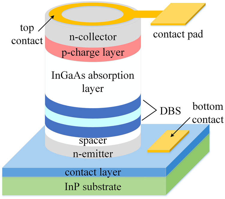
The structure of the detector is shown in Fig. 1. The heterostructure layers are grown on silicon-doped InP substrate by molecular beam epitaxy. The collector and emitter consist of 100 nm with an n-type doping concentration of . The absorption layer consists of 500 nm intrinsic , the absorption wavelength of which is mainly 1–1.6 μm. 1.4 nm AlAs, 6 nm , and 1.4 nm AlAs are grown on the absorption layer forming the DBS for electron tunneling. AlAs is not lattice matched to , but the thickness of the AlAs barrier layer is very thin, which does not induce defects in the epitaxy layer. A 15 nm spacer layer is grown between the DBS and the emitter to prevent scattering from the emitter to the DBS. 30 nm p-charge layer with a doping concentration of is grown between the collector and the absorption layer to modulate the band energy of the detector. Samples of the detectors are fabricated by molecular beam epitaxy. Circle mesas with a diameter of 25 μm are etched by inductively coupled plasma. Ti/Pt/Au ring contacts are deposited on the top of the emitter to form clear apertures with a diameter of 23 μm.
Figure 1.Structure of the detector. The absorption layer consists of 500 nm intrinsic and the DBS consists of 1.4 nm AlAs, 6 nm and 1.4 nm AlAs. A 30 nm p-charge layer with doping concentration of is added to modulate the band energy of the detector.
The incident light within the absorption wavelength of is absorbed by the absorption layer generating electron-hole pairs. When the detector is under a positive bias, the photo-generated holes drift to the DBS and accumulate between the interface of the DBS and the absorption layer. The accumulated holes will lower the band energy of the DBS and enhance the electron tunneling across the DBS, which finally results in an increment of the tunneling current.
Figure 2 shows the simulated band energy variation of the detector after adding the p-charge layer. In the simulation, the bias voltage of the detector is set at 0.2 V. It is shown that after adding the p-charge layer the band energy of the absorption layer rises, but the band energy of the DBS is not changed.
Figure 2.Simulated band energy variation of the detector after adding the p-charge layer. The bias voltage of the detector is set at 0.2 V.
Figure 3 shows the dark current lowering mechanism. For clarity, the thickness of each layer is not proportional to their real value. The current in region S1 comes from the electrons tunneling through the DBS and hot electrons emission over the DBS. According to the band energy simulation, the band energy of the detectors without and with the p-charge layer remain the same within region S1, so the transmission coefficient of the DBS also remains the same. As a result, the sum of the tunneling electrons and hot electrons passing through region S1 of the detector without and with the p-charge layer is equal. When electrons come into region S2, they drift to the collector under the electric field, which generates current in region S2. The dark current density in region S2 can be calculated by[19]where is the dark current density of the detector without the p-charge layer and is the dark current density of the detector with the p-charge layer. and are the conduction band bending of the absorption layer of the detectors without and with the p-charge layer, where and . is the electron charge, is the electron mass, is Boltzman’s constant, is the temperature, and is the bias voltage. Therefore, the dark current density ratio between the detectors with and without the p-charge layer is as and , and , so , that is .
Figure 3.Dark current lowering mechanism. For clarity, the thickness of each layer is not proportional to their real value.
According to the analysis above, the electron transport in region S2 is suppressed after adding the p-charge layer. The accumulated electrons in region S2 will make the band energy of the DBS rise, which in turn suppresses the electron transport through region S1. This process will come to dynamic equilibrium and the dark current density of the detector will reache a steady state. The increment of the band energy of the DBS makes the ground state level of the quantum well increase so that a higher bias voltage is needed for energy alignment between free electrons and the ground state level. Therefore, under certain bias voltages, the responsivity will decrease after adding the p-charge layer.
Figure 4 shows the tested dark current density of the detectors. Samples of the detector without a p-charge layer are also fabricated and tested. The dark current density of the detector without a p-charge layer is at 0.25 V, while that of the detector with a p-charge layer is . The dark current density is reduced by about 3 orders of magnitude after adding the p-charge layer.
Figure 4.Tested dark current density of the detectors. The diameter of the circle mesa is 25 μm.
The photo response of the detector is tested at room temperature, as shown in Fig. 5. A blackbody is used as the light source. The temperature of the blackbody is set at 1073 K and the emergent light is filtered by a light filter with a central wavelength around 1500 nm and a bandwidth of 1000 nm. The detector is placed in front of the blackbody at a linear distance of 12 cm. The position of the detector is adjusted to ensure that the light is incident on the photosensitive area uniformly. The blackbody has five different clear apertures with diameters of 6.4, 9.5, 12.7, 15.9, and 22.2 mm. The power of the emergent light can be controlled by changing the clear aperture of the blackbody. It can be seen from Fig. 5 that the current of the detector increases under light and the current variation has a positive correlation with the power of the incident light.
Figure 5.Photo-response of the detector. The temperature of the blackbody is set at 1073 K and the emergent light is filtered by a light filter with a central wavelength around 1500 nm and a bandwidth of 1000 nm. The detector is placed in front of the blackbody with a linear distance of 12 cm.
Figure 6 shows the calculated responsivity of the detector. It is shown that the responsivity of the detector increases with the increment of the bias voltage. The responsivity reaches 6000 A/W at 0.4 V, when the power of the incident light is 0.7 nW. Meanwhile, the responsivity decreases while the power of the incident light increases. This phenomenon results from the detecting mechanism of the detector. Under strong light illumination, the accumulated holes will not always accumulate near the interface of the DBS and the absorption layer, but will keep a distance away from it due to the lowering of the energy level of the DBS and the repulsive force of the accumulated holes. Therefore, the tunneling current enhancement effect will be weakened as the band modulation effect is weaker when the accumulated holes keep a distance away from the DBS. Actually, according to our previous research[20], the relationship between the responsivity () and the power of the incident light () is simulated to be where and are constant numbers. Their values depend on the working temperature of the detector, the thickness of the absorption layer and the DBS, and the photosensitive area of the detector.
To test the time-resolved photocurrent of the detector, a laser working at 1550 nm with a power of 5 mW is used as the light source. The power of the laser light is further attenuated to 50 pW by connecting optical fiber attenuators to the optical fiber. The frequency of the laser is set at 5 kHz and the bias voltage of the detector is set at 0.29 V. The output signal is first amplified by an amplifier, then the signal is measured by an oscilloscope. Figure 7 shows the time-resolved photocurrent of the detector at room temperature. It is shown that periodic photocurrent pulses are generated that coincide with the frequency of the laser pulses. The rise time and fall time are 60 and 66 μs, respectively.
Figure 7.Time-resolved photocurrent of the detector at room temperature. The frequency of the laser pulses is 5 kHz and the bias voltage of the detector is 0.29 V.
To evaluate the weak light detection capability of the detector, the noise equivalent power (NEP) should be tested. The NEP is the signal power that gives a signal-to-noise ratio of 1 in a 1 Hz output bandwidth, and it can be calculated by where and are the root mean square (RMS) signal voltage and the RMS noise voltage of the detector, respectively.
The NEP testing system is basically the same as the time-resolved photocurrent testing system, but the oscilloscope is replaced by a spectrum analyzer. The incident power on the photosensitive area of the detector is 50 pW and the frequency of the laser pulses is 5 kHz. The amplification factor of the amplifier is 500. The central frequency and bandwidth of the spectrum analyzer are set at 5 and 3 kHz, respectively. Figure 8 shows the RMS signal voltage and the RMS noise voltage of the detector. The RMS signal voltage of the detector at 5 kHz is 1.3 mV. The RMS noise voltage of the detector is calculated by where is the sampling number during the noise voltage test. In this way, the RMS noise voltages of the detector is calculated to be . So the NEP of the detector at 5 kHz is . The normalized detectivity is calculated to be .
Figure 8.RMS signal voltage and RMS noise voltage of the detector. The incident power on the photosensitive area of the detector is 50 pW and the frequency of the laser pulses is 5 kHz.
In conclusion, SWIR detectors combining a AlAs/InGaAs/AlAs DBS with an InGaAs absorption layer are fabricated by molecular beam epitaxy. By adding a p-charge layer, the dark current density of the detector is lowered by 3 orders of magnitude, which makes the detector suitable for composing large-scale detector arrays. The dark current density can be further reduced by adding a thicker p-charge layer, but the responsivity and working frequency of the detector will also be reduced. The responsivity of the detector reaches 6000 A/W at 0.4 V, when the power of the incident light is 0.7 nW. While illuminating the detector by a laser working at 5 kHz, periodic photocurrent pulses are generated that coincide with the frequency of the laser pulses. The NEP of the detector at 5 kHz is . The detector is promising for achieving room temperature single-photon sensitivity by restricting the area of the DBS region to .