
Bingxin Kang, Yi Cai, Lingxue Wang. External quantum efficiency-enhanced PtSi Schottky-barrier detector utilizing plasmonic ZnO:Al nanoparticles and subwavelength gratings[J]. Chinese Optics Letters, 2016, 14(7): 070401
- Chinese Optics Letters
- Vol. 14, Issue 7, 070401 (2016)
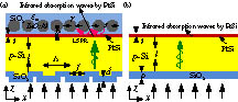
Fig. 1. Schematic of (a) proposed and (b) conventional PtSi SBD structure.
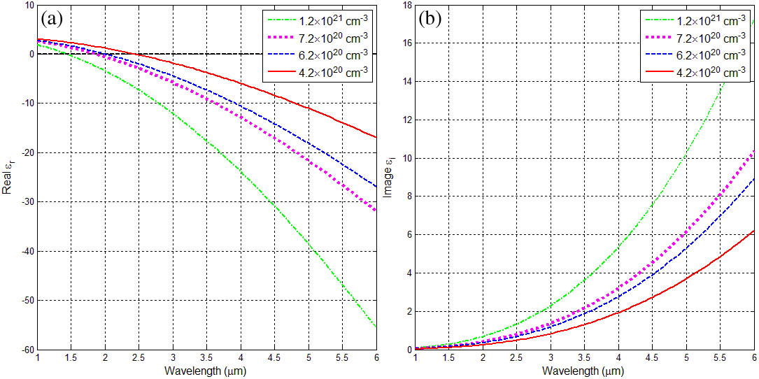
Fig. 2. (a) Real and (b) imaginary components of complex permittivity of ZnO:Al material with different electron concentrations.
Fig. 3. Quality factors versus wavelength for ZnO:Al, silver, and gold materials. Inset of the figure shows the ε i
Fig. 4. Absorption efficiency for (a) different ZnO:Al nanoparticle radii r p = 0.4 μm p r = 0.65 μm
Fig. 5. Simulated electric field distributions around nanoparticles at the two peak wavelengths of (a) 3.5 and (b) 4.6 μm in Fig. 4(a) , with r = 0.65 μ m p = 0.4 μ m
Fig. 6. Absorption efficiencies of conventional SBD structures with and without nanoparticles, and that of the proposed structure.
Fig. 7. Theoretical EQE by our proposed structure compared to the conventional structure. The EQEs of the measurements from the literature and the theoretical limit (A ( λ ) = 1
|
Table 1. Optimized Parameters for Simulating Proposed PtSi SBD Structure Performance.

Set citation alerts for the article
Please enter your email address
© Copyright 2018-2021 | Chinese Laser Press. All Rights Reserved 沪ICP备15018463号-20