School of Optoelectronics, Beijing Institute of Technology, Key Laboratory of Photoelectronic Imaging Technology and Systems, Beijing Engineering Research Centre for Mixed Reality and Advanced Display Technology, Beijing 100081, China
A infrared light trapping structure combining front subwavelength gratings and rear ZnO:Al nanoparticles for a PtSi Schottky-barrier detector over a 3–5 μm waveband is theoretically investigated. By selecting the proper plasmonic material and optimizing the parameters for the proposed structure, the absorption of the PtSi layer is dramatically improved. The theoretical results show that this improvement eventually translates into an equivalent external quantum efficiency (EQE) enhancement of 2.46 times at 3–3.6 μm and 2.38 times at 3.6–5 μm compared to conventional structures. This improvement in the EQE mainly lies in the increase of light path lengths within the PtSi layer by the subwavelength grating diffraction and nanoparticle-scattering effects.
Silicide Schottky-barrier detectors (SBDs) have the potential for over 100 M-pixels resolution infrared focal plane arrays (FPAs) due to their integrability with Si CCDs in the 3–5 μm waveband. SBD has a typical 2–8 nm thin metal-silicide (PtSi) active layer to increase the probability of internal photoemission, whereas external quantum efficiency (EQE) becomes relative low due to poor absorption[1,2]. To circumvent this, an optical cavity (e.g., rear mirror) is commonly put inside PtSi SBDs to create a standing wave in the PtSi active layer[3,4]. Additionally, other efficient infrared light-trapping schemes are required to increase the optical path length within the PtSi layer. These schemes include photonic crystals[5] and porous structures[6,7], black silicon, and moth-eye light-trapping nanostructures[8–11]. Photonic crystals and porous structures involving texturing the PtSi active layer usually degrade the electrical performance of PtSi SBD. Black silicon and moth-eye structures of PtSi in Refs. [8,9] improved the absorption mainly in the 1–2.5 μm shortwave-infrared wavelength range.
Metallic nanoparticles, which support localized surface plasmons (LSP), have been used as the front or back structures of solar cells to enhance the light path lengths by forward or backward scattering, respectively[12–17]. Motivated by solar cells, we propose a plasmonic nanoparticle back-scattering reflector together with a front antireflection (AR) -film-coated subwavelength grating as a hybrid infrared light-trapping structure without interfering with the electrical properties to enhance the absorption of PtSi film over a 3–5 μm waveband. The nanoparticle structures behind the PtSi layer act as a strong rear reflector, utilizing LSP in the form of electron oscillations at the surface of the nanoparticles to significantly enhance the infrared light absorption in the PtSi layer by the light scattering at larger angles from a high scattering cross section. The AR -film-coated subwavelength gratings positioned on the Si substrate side are intended to reduce the reflection and diffract the incident infrared light into higher angles of propagation. The absorption enhancement mechanism of PtSi SBD with only a subwavelength grating on the front has been demonstrated in theory and experimentally by us. A Letter has been submitted to Optical Engineering. So the detailed analysis of AR -film-coated subwavelength grating is not discussed here except to give the optimized parameters of the grating used in this Letter.
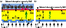
The proposed PtSi SBD structure is shown in Fig. 1(a), and the conventional structure is in Fig. 1(b) for comparison. It is a stack composed of a -film-coated subwavelength grating as an incident plane on an Si substrate, a formed PtSi film used as the active layer, where infrared absorption generates hot carriers that are eventually separated at the Schottky junction and emitted into the Si substrate. The rear surface of the PtSi film is patterned as a nanoparticle array embedded in an dielectric. For a conventional PtSi detector, the proper PtSi film thickness is 0.003 μm, the AR film thickness is 0.6 μm, and the p-type Si thickness is 450 μm. Because the Si substrate () is nearly transparent and its loss is close to zero in the 3–5 μm waveband, we simply set to 2 μm to reduce the simulation time, and the results are not affected. and are used in our proposed PtSi SBD structure. The other parameters of the proposed structure are defined as follows: and are the radius and pitch of nanoparticles, and is the distance of spacing barrier layer between the nanoparticles and the PtSi film, avoiding PtSi film metallic impurity and providing beneficial infrared light-coupling space with its proper value. , , and represent the period, groove depth, and fill factor of the subwavelength grating, and is the thickness of the subwavelength grating. The optical constants of [18] and PtSi[19] were given. The electromagnetic wave propagation was investigated by the finite-difference time-domain method and a rigorous coupled-wave analysis using Rsoft software. By optimizing the above parameters, the optimal absorption efficiency can be calculated.
Sign up for Chinese Optics Letters TOC. Get the latest issue of Chinese Optics Letters delivered right to you!Sign up now
Figure 1.Schematic of (a) proposed and (b) conventional PtSi SBD structure.
In the search for potential plasmonic materials in the 3–5 μm waveband range to integrate nanostructures within PtSi SBD, conventional plasmonic metals (Au or Ag), highly doped semiconductors, graphene[20,21], and highly doped transparent conducting oxides (TCOs)[22–25] are extensively investigated. The localized surface plasmons resonance (LSPR) of Au or Ag nanostructures (nanoshell, nanorod, or nanocage) can be tuned to the 3–5 μm waveband region, while excessive optical losses make them less suitable for PtSi SBD[20]. Due to the difficulty in increasing the carrier concentration further, highly doped semiconductors materials cannot be plasmonic (i.e., exhibiting metallic properties) for wavelengths shorter than 5.5 μm[26–28]. Graphene is a good plasmonic material for terahertz but not for infrared applications, according to the initial theoretical estimates. Although indium tin oxide (ITO) and gallium zinc oxide (GZO) of TCOs have plasma wavelength values of approximately 1.3–3.5 μm[29,30], they are apt to form amorphous films, resulting in lower carrier mobility and more losses[31]. Zinc oxide doped with aluminum (ZnO:Al) of TCOs exhibits metallic optical properties beyond 1.8 μm, and these properties can be tuned by controlling the Al doping[32]. They have smaller losses and small negative real parts of the complex permittivity and therefore are suitable for PtSi SBD over the 3–5 μm waveband. Meanwhile, ZnO:Al films can be easily fabricated by typical pulsed-laser-deposition or radio-frequency magnetron sputtering techniques.
The optical properties of ZnO:Al can be characterized in terms of Drude’s theory[33,34], We plot the real () and imaginary () parts of the dielectric constant of the ZnO:Al material from 1 to 6 μm for different electron concentrations[35], as shown in Figs. 2(a) and 2(b). Both and are significantly smaller than those of gold or silver[36]. The negative of the ZnO:Al material should be approximately double that of the surrounding dielectric to support LSPR modes by ZnO:Al nanoparticles in the 3–5 μm infrared band. The permittivity of the surrounding medium is 2.1. Therefore, the electron concentration value of is adopted, and the losses () under this concentration are smaller than others.
Figure 2.(a) Real and (b) imaginary components of complex permittivity of ZnO:Al material with different electron concentrations.
Figure 3 show the quality factor [20] of the LSPR system for the ZnO:Al material as a function of the wavelength and compared with silver and gold nanostructures ( of these materials is shown in inset). Despite the fact that the values of ZnO:Al are obviously lower than silver and gold nanostructures in the 3–5 μm waveband, ZnO:Al can exhibit absorption losses that are tens or even hundreds of times lower than that of the silver and gold shown in inset. Furthermore, as the diameter of ZnO:Al is larger than silver or gold atoms, ZnO:Al atoms cannot penetrate through the dielectric layer to form an electrical connection with the PtSi film and destroy the SBD structure.
Figure 3.Quality factors versus wavelength for ZnO:Al, silver, and gold materials. Inset of the figure shows the of ZnO:Al, silver, and gold materials. Note: ZnO:Al can exhibit absorption losses tens or hundreds of times lower than those of silver and gold.
When finished with the material choice of nanoparticles, we begin to investigate conventional structure with only ZnO:Al nanoparticles on the rear. Here, the nanoparticle pitch is assumed to 1.5 μm to match the grating period. Figures 4(a) and 4(b) show its absorption efficiency for different and compared to the conventional structure. In Fig. 4(a), the increased of the nanoparticle leads to the increase of the absorption efficiency due to the larger scattering cross section. In addition, nanoparticles will broaden the absorption spectrum as a result of the multimode radiation-stimulated resonance. In Fig. 4(b), increased results in a gradual shift of the absorption efficiency peak towards longer wavelengths, on account of the increased optical thickness of the Fabry–Perot cavity. This is beneficial for improving the absorption of longer wavelengths. As shown in Fig. 4, the optimum and in order to maximize the absorption efficiency are 0.65 and 0.4 μm, respectively. The optimized parameters of the nanoparticles are all shown in Table 1.
Parameters
Symbol
Value (μm)
Parameters
Symbol
Value (μm)
PtSi film thickness
t
0.003
Thickness of SiO2 subwavelength grating
d
0.4
p-type Si thickness
l
2
Subwavelength-grating fill factor
f
0.5
SiO2 AR film thickness for conventional PtSi detector
Figure 4.Absorption efficiency for (a) different ZnO:Al nanoparticle radii with the distance between the nanoparticles and the PtSi layer , and for (b) different with .
Figures 5(a) and 5(b) show the simulated electric field distributions around the nanoparticles (pink circles) at the two peak values of 3.5 and 4.6 μm determined in Fig. 4(a), respectively. The PtSi layer is located at 2.5 μm along the -axis. LSPRs are excited around the ZnO:Al nanoparticles that can be seen in Fig. 5. There are Bloch mode-like diffraction patterns with a periodicity in the horizontal -direction under the both wavelength of 3.5 and 4.6 μm. The far-field interaction of the scattered field in the 4.6 μm-long wavelength seems more intensive than in 3.5 μm and displays a continuously stronger light-gathering band around the PtSi layer. As expected, the absorption efficiency of the PtSi layer measured by the Rsoft absorption monitor is 85% in 4.6 μm, and the value is 72% in 3.5 μm. Though the infrared light is confined close to the ZnO:Al nanoparticles’ surface, absorption can primarily occur within the PtSi film due to the higher optical scattering cross section offered by the nanoparticles.
Figure 5.Simulated electric field distributions around nanoparticles at the two peak wavelengths of (a) 3.5 and (b) 4.6 μm in Fig. 4(a), with and , respectively.
The optimized parameters of the subwavelength grating are shown in Table 1. Figure 6 gives the absorption efficiency of the combined PtSi SBD structure utilizing optimized rear ZnO:Al nanoparticles and front subwavelengths. For comparison, the absorption efficiencies of the conventional SBD structure with and without nanoparticles are also shown. The absorption efficiency of the conventional structure lies between 20% and 38%. Two not very obvious absorption peaks occur at and 4.6 μm. However, when the ZnO:Al nanoparticles are added, the absorption efficiency is increased and the range is expanded from 28% to 85%. The two absorption peaks observed in the conventional structure exhibit sharper profiles, and the 3.4 μm peak shifts to 3.5 μm. In the case of the proposed structure, however, the two absorption peaks disappear and the whole absorption spectrum is shown with a complex, irregular shape. The difference in the absorption efficiency between the proposed structure and conventional structure with particles indicates that both the ZnO:Al nanoparticles and subwavelength grating contribute to infrared light absorption and make no obvious wavelength selectivity due to their interaction with each other. In addition, the interaction between nanoparticles and gratings broadens the spectral response range and leads to absorption enhancement in most ranges of wavelengths compared to the conventional structure. The absorption efficiency increases evenly and the average absorption efficiency over the 3–5 μm waveband is approximately 80%. The average absorption efficiency in the 4–5 μm waveband is even larger than 85%.
Figure 6.Absorption efficiencies of conventional SBD structures with and without nanoparticles, and that of the proposed structure.
Finally, we measure and compare the EQE of the proposed PtSi SBD with that of the conventional structure. The EQE of SBD[37] is defined by , where and are the absorption efficiency and the thickness of PtSi, is Planck’s constant, is the frequency of infrared radiation, is a constant for any given value of , is the mean free path of the hot carrier, and is the Schottky-barrier height in eV. Thus, we model the theoretical EQE on the basis of the simulated . The Schottky-barrier height value is taken to 0.208 eV, as measured by Elabd and Kosonocky[37] under the same PtSi film thickness of 0.003 μm as ours, and the mean free path is taken as the typical value of 80 nm[8]. Figure 7 shows the EQE of the proposed PtSi SBD (blue dashed line) and conventional structure (red dashed line) in 3–5 μm. For comparison, the theoretical limiting ) (black solid line) and measured EQE of PtSi SBD with the optical cavity by Elabd and Kosonocky (black dashed line) are also shown. We can see that the proposed PtSi SBD dramatically improves the EQE, having a maximum value of 20% at 3.1 μm. Compared to conventional structure, the proposed PtSi SBDs have an average EQE enhancement factor of 2.46 at 3–3.6 μm and 2.38 at 3.6–5 μm. For measurements from literature, the proposed PtSi SBDs have an average EQE enhancement factor of 1.8 at 3–3.6 μm and 1.25 at 3.6–5 μm. The sensitivity of the SBD FPAs is improved by a factor of 1.69 through integrating infrared light energy over the 3–5 μm waveband.
Figure 7.Theoretical EQE by our proposed structure compared to the conventional structure. The EQEs of the measurements from the literature and the theoretical limit () are also shown.
While the PtSi SBD is made into an FPA, its sensitivity can be described by noise-equivalent temperature difference (). The relationship between and EQE is deduced as where is the pixel area, is the array fill factor, is the sensor time frame, is the -number, is the atmospheric transmittance, is the optical transmittance, is the background temperature, is the resulting noise, and and are the cut-on and cut-off wavelengths. NETD measured in Ref. [35] is 100 mK. Based on the above parameters, the of our proposed PtSi SBD has reduced by 41%.
In conclusion, a proposed 3–5 μm waveband EQE-enhanced PtSi SBD structure, based on the interaction with ZnO:Al nanoparticles and subwavelength gratings located on the rear and front sides of the structure is demonstrated. Our results show that the proposed structure offers a promising way to enhance the absorption efficiency and to improve the EQE further. The absorption enhancement is due to scattering via radiation-stimulated resonance, which is aided by the conduction electrons of the ZnO:Al nanoparticles, along with the increase of effective optical path within the active layer by AR effects and the forward scattering of the incident infrared radiation in the -film-coated subwavelength grating. The theoretical EQE of the proposed PtSi SBD and of its FPAs are significantly improved and compared with measurements from Ref. [38]. The improvement of the EQE is exciting for integrating SBDs with CCDs of over 100 M pixels. We believe that these techniques are also applicable to other Schottky-barrier systems such as metal-GaAs and metal- and metal-silicide Si structures.