• Advanced Photonics Nexus
  • Vol. 1, Issue 2, 024001 (2022)
Renlong Zhou1, Kaleem Ullah2, Naveed Hussain3, Mohammed M. Fadhali4、5, Sa Yang1, Qiawu Lin1, Muhammad Zubair6, and Muhammad Faisal Iqbal7、8、*
Author Affiliations
  • 1Guangdong University of Education, School of Physics and Information Engineering, Guangzhou, China
  • 2University of Delaware, Department of Electrical and Computer Engineering, Newark, Delaware, United States
  • 3University of California, Department of Electrical Engineering and Computer Science, Irvine, California, United States
  • 4Jazan University, Faculty of Science, Department of Physics, Jazan, Saudi Arabia
  • 5Ibb University, Faculty of Science, Department of Physics, Ibb, Yemen
  • 6Institute of Energy and Climate Research, Materials Synthesis and Processing (IEK-1), Forschungszentrum Jülich GmbH, Jülich, Germany
  • 7University of Science and Technology of China, Hefei National Laboratory for Physical Sciences at the Microscale, Hefei, China
  • 8Riphah International University Faisalabad, Department of Physics, Faisalabad, Pakistan
  • show less
    DOI: 10.1117/1.APN.1.2.024001 Cite this Article Set citation alerts
    Renlong Zhou, Kaleem Ullah, Naveed Hussain, Mohammed M. Fadhali, Sa Yang, Qiawu Lin, Muhammad Zubair, Muhammad Faisal Iqbal. Recent advances in photonics of three-dimensional Dirac semimetal Cd3As2[J]. Advanced Photonics Nexus, 2022, 1(2): 024001 Copy Citation Text show less
    Crystal structure, projections of the 3D Dirac fermions, and refractive index of 3D DSM. (a) Cd3As2′s nonprimitive tetragonal unit cell is made up of 24 slightly deformed antifluorite cells with two cadmium vacancies. 96 cadmium atoms and 64 arsenic atoms are contained in this cell. (b) The real and imaginary components of dynamic conductivity in 3D DSMs. (c) Schematic representation of the projected Dirac cone into the (kx, ky, E) space reconstructed from experimental values. The red lines show the linear dispersions along the kx and ky axes. (d) Stacking plots of constant-energy contours at different binding energies reveal the structure of the Dirac cone band. The red dotted lines serve as visual cues for the dispersions and intersect at the Dirac point. (e) A three-dimensional intensity plot of the photoemission spectrum at the Dirac point, demonstrating identical cone-shaped dispersion to that in (c). The figure is reproduced with the permission of (a) Ref. 34 © 2018 American Physical Society, (b) Ref. 35 © 2016 American Physical Society, and (c)–(e) Ref. 3 © 2018 Nature Publishing Group.
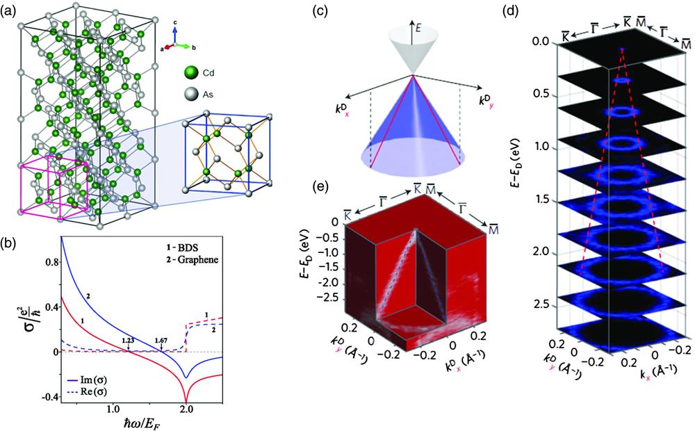
    Fig. 1. Crystal structure, projections of the 3D Dirac fermions, and refractive index of 3D DSM. (a) Cd3As2s nonprimitive tetragonal unit cell is made up of 24 slightly deformed antifluorite cells with two cadmium vacancies. 96 cadmium atoms and 64 arsenic atoms are contained in this cell. (b) The real and imaginary components of dynamic conductivity in 3D DSMs. (c) Schematic representation of the projected Dirac cone into the (kx, ky, E) space reconstructed from experimental values. The red lines show the linear dispersions along the kx and ky axes. (d) Stacking plots of constant-energy contours at different binding energies reveal the structure of the Dirac cone band. The red dotted lines serve as visual cues for the dispersions and intersect at the Dirac point. (e) A three-dimensional intensity plot of the photoemission spectrum at the Dirac point, demonstrating identical cone-shaped dispersion to that in (c). The figure is reproduced with the permission of (a) Ref. 34 © 2018 American Physical Society, (b) Ref. 35 © 2016 American Physical Society, and (c)–(e) Ref. 3 © 2018 Nature Publishing Group.
    Experimental methodologies to grow Cd3As2 nanostructures, thin films, single crystals, and fabrication of Cd3As2-based devices. (a) Schematic diagram of nucleation and growth process of Cd3As2 nanostructures by PVD. (b) Flow diagram of CVD growth of nano-wires. (c) Display of Cd3As2/organic thin films based device fabricated by MBE, showing excellent flexibility. (d) Schematic diagram of pulsed laser deposition technique to grow Cd3As2 thin films. (e) Graphene/Cd3As2 based heterostructure device fabricated by the CVD method. (f) SSVG system to grow single crystal Cd3As2. The figure is reproduced with the permission of (a) Ref. 44 © 2015 American Physical Society, (b) Ref. 50 © 2021 Springer Nature, (c) Ref. 46 © 2019 American Physical Society, (d) Ref. 51 © 1984 Elsevier, (e) Ref. 52 © 2021 Wiley-VCH GmbH, and (f) Ref. 53 © 2015 Nature Publishing Group.
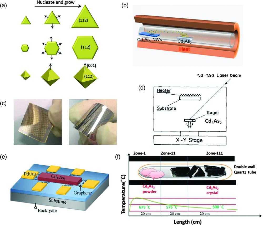
    Fig. 2. Experimental methodologies to grow Cd3As2 nanostructures, thin films, single crystals, and fabrication of Cd3As2-based devices. (a) Schematic diagram of nucleation and growth process of Cd3As2 nanostructures by PVD. (b) Flow diagram of CVD growth of nano-wires. (c) Display of Cd3As2/organic thin films based device fabricated by MBE, showing excellent flexibility. (d) Schematic diagram of pulsed laser deposition technique to grow Cd3As2 thin films. (e) Graphene/Cd3As2 based heterostructure device fabricated by the CVD method. (f) SSVG system to grow single crystal Cd3As2. The figure is reproduced with the permission of (a) Ref. 44 © 2015 American Physical Society, (b) Ref. 50 © 2021 Springer Nature, (c) Ref. 46 © 2019 American Physical Society, (d) Ref. 51 © 1984 Elsevier, (e) Ref. 52 © 2021 Wiley-VCH GmbH, and (f) Ref. 53 © 2015 Nature Publishing Group.
    OHG in 3D DSM Cd3As2. (a) Schematic demonstration of the generation of HHG from 3D DSM thin film. (b) Room temperature HHG in Cd3As2 film and air. (c) Theoretically estimated HHG in a 3D DSM thin film when a linearly polarized pulse with a central frequency of 1 THz and a peak field intensity of 10 MV/m generates harmonics up to the 31st order and beyond with energy conversion efficiency far over 10−5. (d) A comparison of the THG signal among the Cd3As2, glass, MoS2, and graphene. The figure is reproduced with the permission of (a) Ref. 33 © 2021 Nature Publishing Group, (b) Ref. 32 © 2020 Nature Publishing Group, (c) Ref. 94 © 2020 American Physical Society, and (d) Ref. 93 © 2020 AIP Publishing.
    Fig. 3. OHG in 3D DSM Cd3As2. (a) Schematic demonstration of the generation of HHG from 3D DSM thin film. (b) Room temperature HHG in Cd3As2 film and air. (c) Theoretically estimated HHG in a 3D DSM thin film when a linearly polarized pulse with a central frequency of 1 THz and a peak field intensity of 10 MV/m generates harmonics up to the 31st order and beyond with energy conversion efficiency far over 105. (d) A comparison of the THG signal among the Cd3As2, glass, MoS2, and graphene. The figure is reproduced with the permission of (a) Ref. 33 © 2021 Nature Publishing Group, (b) Ref. 32 © 2020 Nature Publishing Group, (c) Ref. 94 © 2020 American Physical Society, and (d) Ref. 93 © 2020 AIP Publishing.
    Plasmonics in 3D DSM. (a) The variation of optical conductivity with a THz frequency in a Cd3As2 thin film. (b) Stripes of Cd3As2 thin film with a transmission spectrum demonstrating plasmonic resonances and an inset illustrating the transmission line model for transmission through a thin film (t≪λ), where intraband conductivity can be modeled as series resistance, R, and kinetic inductance, Lk, which provides the Drude dispersion. (d) The distribution of the electric field at the z direction in a proposed PIT system at frequency of 1.335 THz. (e) Transmission spectra of a patterned stripe array showing plasmonic resonances for a Cd3As2 thin film whose dimensions are presented in the inset of this figure. (f) A comparison of surface plasmon propagation lengths between different plasmonic waveguides. The figure is reproduced with the permission of (a)–(c) and (e) Ref. 100 © 2019 American Chemical Society, (d) Ref. 105 © 2017 Optical Society of America, and (f) Ref. 19 © 2019 AIP Publishing.
    Fig. 4. Plasmonics in 3D DSM. (a) The variation of optical conductivity with a THz frequency in a Cd3As2 thin film. (b) Stripes of Cd3As2 thin film with a transmission spectrum demonstrating plasmonic resonances and an inset illustrating the transmission line model for transmission through a thin film (tλ), where intraband conductivity can be modeled as series resistance, R, and kinetic inductance, Lk, which provides the Drude dispersion. (d) The distribution of the electric field at the z direction in a proposed PIT system at frequency of 1.335 THz. (e) Transmission spectra of a patterned stripe array showing plasmonic resonances for a Cd3As2 thin film whose dimensions are presented in the inset of this figure. (f) A comparison of surface plasmon propagation lengths between different plasmonic waveguides. The figure is reproduced with the permission of (a)–(c) and (e) Ref. 100 © 2019 American Chemical Society, (d) Ref. 105 © 2017 Optical Society of America, and (f) Ref. 19 © 2019 AIP Publishing.
    Ultrafast photocarrier dynamics in 3D DSM: Cd3As2. (a) Schematic representation of the excitation and relaxation of electrons and holes from process 1 to 5 (1. before excitation, 2. immediately after excitation, 3. high-temperature thermal distribution, 4. partially cooled distribution with inverted populations, 5. a partially cooled, noninverted distribution). (b) The Cd3As2 sample structure is shown schematically with the illustration of optical pump THz probe spectroscopy. (c) The modulation depth (MD) at 1.0 THz versus pump fluences of Cd3As2 thin film at room temperature. The figure is reproduced with the permission of (a) Ref. 133 © 2017 AIP Publishing, (b) Ref. 113 © 2019 AIP Publishing, and (c) Ref. 23 © 2021 Wiley-VCH GmbH.
    Fig. 5. Ultrafast photocarrier dynamics in 3D DSM: Cd3As2. (a) Schematic representation of the excitation and relaxation of electrons and holes from process 1 to 5 (1. before excitation, 2. immediately after excitation, 3. high-temperature thermal distribution, 4. partially cooled distribution with inverted populations, 5. a partially cooled, noninverted distribution). (b) The Cd3As2 sample structure is shown schematically with the illustration of optical pump THz probe spectroscopy. (c) The modulation depth (MD) at 1.0 THz versus pump fluences of Cd3As2 thin film at room temperature. The figure is reproduced with the permission of (a) Ref. 133 © 2017 AIP Publishing, (b) Ref. 113 © 2019 AIP Publishing, and (c) Ref. 23 © 2021 Wiley-VCH GmbH.
    Perfect absorption using 3D DSM and some other photonic properties. (a) A schematic of the perfect absorber composed of a patterned 3D DSM film, the dielectric layer, and a metal reflector. (b) Calculated electric field distribution of a crossed shape absorber composed of 3D DSM. (c) Simulated absorption of a metamaterial absorber based on 3D DSM. (d) Measured reflectivity of Cd3As2 at various temperatures. The reflectance of gold was used to normalize all measurements. (e) and (f) Static photoemission electron microscopic (PEEM) image of fabricated Cd3As2 nanostructures excited by a linear-polarized 410 nm laser pulse (e) and circularly polarized light (f). The polarization is manifested by the red arrow. (g) Reflection amplitude of a coding unit cell of 0 and 1 of metasurface made with 3D DSM. The figure is reproduced with the permission of (a) Ref. 154 © 2019 Optical Society of America (OSA), (b) Ref. 158 © 2021 MDPI, (c) Ref. 156 © 2018 Optical Society of America (OSA), (d) Ref. 16 © 2020 Wiley-VCH GmbH, (e) and (f) Ref. 164 © 2022 Wiley-VCH GmbH, and (g) Ref. 165 © 2022 Elsevier.
    Fig. 6. Perfect absorption using 3D DSM and some other photonic properties. (a) A schematic of the perfect absorber composed of a patterned 3D DSM film, the dielectric layer, and a metal reflector. (b) Calculated electric field distribution of a crossed shape absorber composed of 3D DSM. (c) Simulated absorption of a metamaterial absorber based on 3D DSM. (d) Measured reflectivity of Cd3As2 at various temperatures. The reflectance of gold was used to normalize all measurements. (e) and (f) Static photoemission electron microscopic (PEEM) image of fabricated Cd3As2 nanostructures excited by a linear-polarized 410 nm laser pulse (e) and circularly polarized light (f). The polarization is manifested by the red arrow. (g) Reflection amplitude of a coding unit cell of 0 and 1 of metasurface made with 3D DSM. The figure is reproduced with the permission of (a) Ref. 154 © 2019 Optical Society of America (OSA), (b) Ref. 158 © 2021 MDPI, (c) Ref. 156 © 2018 Optical Society of America (OSA), (d) Ref. 16 © 2020 Wiley-VCH GmbH, (e) and (f) Ref. 164 © 2022 Wiley-VCH GmbH, and (g) Ref. 165 © 2022 Elsevier.
    Schematic shows the potential applications that can generate with the photonics of 3D DSM Cd3As2.
    Fig. 7. Schematic shows the potential applications that can generate with the photonics of 3D DSM Cd3As2.
    MaterialPreparation methodPrecursor/targetGrowth temperatureSubstrateReference
    Cd3As2 thin filmPLDMixture of 6N5 Cd and 7N5 As shots targetRoom temperatureSrTiO3Ref. 45
    Cd3As2 thin filmPLDSingle crystal Cd3As2 targetRoom temperatureFused quartz platesRef. 51
    Cd3As2 nanostructuresPVDCd3As2 powder650°CSiO2/SiRef. 44
    Cd3As2 thin filmMBECd3As2 bulk170°CMicaRef. 21
    Cd3As2 thin filmMBECd3As2 target140°CCdTeRef. 60
    Cd3As2 thin filmMBECd3As2 target150°C to 170°CGaAsRef. 49
    Cd3As2 thin filmMBECd3As2 target180°CGaAs (111)BRef. 61
    Cd3As2 nanostructuresCVD/ vapor solid mechanismCd3As2 powder760°C SiRef. 47
    Cd3As2 nano-beltsCVDCd3As2 powder760°CQuartzRef. 52
    Cd3As2 microbeltsCVDCd3As2 powder760°CSiRef. 58
    Cd3As2 submicron wiresCVDCd3As2 powder (6N pure)Upstream: 650°C Downstream: 350°CSiO2/Si coated with L BiI3/ ethanol solutionRef. 62
    Cd3As2 single crystalsCVDCd and As powders825°CRef. 63
    Cd3As2 single crystalsSSVGStoichiometric mixture of Cd and As elements850°CRef. 53
    Table 1. Growth conditions for Cd3As2 thin films, nanostructures, and single crystals for various growth techniques.
    Sr. NoFabrication techniqueAdvantageDisadvantageReference
    1Molecular beam epitaxy1. Deposition is carried out in ultrahigh vacuum (up to 1010mbar).1. It causes poor crystallinity of material (Cd3As2) due to low growth temperature.Refs. 45, 46, 64, 65
    2. High-quality large-area epitaxial Cd3As2 thin films can be grown with controlled thickness.
    3. Good capacity to produce Cd3As2 heterostructures and superlattices with abrupt interfaces.
    2Pulse laser deposition1. Suitable for the growth of materials (Cd3As2) with high melting points, complicated stoichiometry, and sandwich architectures.1. It causes nonuniformity of particulate size across the surface of Cd3As2 films due to the presence of molten material in the ablated material.Refs. 45, 55, 6567
    2. Can be operated in both inert and ultrahigh vacuum. High deposition rates and takes short time for deposition.2. There is a possibility of splashing and formation of microsized island on the surface of deposited film.
    3Chemical vapor deposition1. Feasible to synthesize both Cd3As2 thin films and nanostructures.1. Limited capacity to produce heterostructures and superlattices of Cd3As2 with abrupt interfaces.Refs. 43, 52, 58
    2. Versatile, adaptable, compatible, simplest, reproducible, productive, and cost effective technique.2. Film thickness is not easy to control.
    3. In CVD, deposition at high temperatures cause stresses in the Cd3As2 thin films and limits the choice of substrates.
    4Physical vapor deposition1. It is suitable to synthesize both Cd3As2 thin films and nanostructures.1. Low deposition rates.Refs. 44, 45, 56
    2. It involves both thermal heating and kinetic ejection of target material.2. Difficulty in evaporating and formation of alloys thin films.
    3. Film thickness control is easy and it is environment friendly and easy to use.3. It is extremely difficult to control stoichiometry of Cd3As2 thin films.
    5Self-selecting vapor growth1. Suitable to grow Cd3As2 single crystals.1. The growth process for Cd3As2 is very slow and deposition can take place a week to form.Refs. 53, 59
    2. It involves little variation in temperature between the evaporation and deposition portions.2. The crystal shape of Cd3As2 is not controllable.
    3. Scale-up beyond 8  cm3 has not been demonstrated.
    Table 2. The advantages and disadvantages of various fabrication techniques for the fabrication of Cd3As2.
    Nonlinear materialReferenceχ(3)/m2V2Phase controlAdvantageDisadvantage
    Traditional bulk material (LiNbO3)Refs. 85, 861021NoCommercially availableWeak nonlinearity
    Plasmonic nanostructures (gold)Refs. 868810181019YesStrong field enhancementHigh losses
    Dielectric nanostructuresRefs. 89 and 901020YesLow lossesModerate field enhancement
    2D materials thin filmsRefs. 69, 91, 9210181019Yes1. Tunable1. Due to atomic thickness the light–matter interaction is weak.
    2. Easily integrated with other bulk structures2. Making nanostructures is difficult
    Cd3As2 thin filmRef. 931019Yes1. TunableNeed to be explored (Very few experimental findings and minimal understanding)
    2. Extendable to other structures
    3. Easy to make nanostructures
    Table 3. Comparison between Cd3As2 nonlinear efficiency with other materials including advantages and disadvantages.
    Renlong Zhou, Kaleem Ullah, Naveed Hussain, Mohammed M. Fadhali, Sa Yang, Qiawu Lin, Muhammad Zubair, Muhammad Faisal Iqbal. Recent advances in photonics of three-dimensional Dirac semimetal Cd3As2[J]. Advanced Photonics Nexus, 2022, 1(2): 024001
    Download Citation