Renlong Zhou1, Kaleem Ullah2, Naveed Hussain3, Mohammed M. Fadhali4,5..., Sa Yang1, Qiawu Lin1, Muhammad Zubair6 and Muhammad Faisal Iqbal7,8,*|Show fewer author(s)
Renlong Zhou, Kaleem Ullah, Naveed Hussain, Mohammed M. Fadhali, Sa Yang, Qiawu Lin, Muhammad Zubair, Muhammad Faisal Iqbal, "Recent advances in photonics of three-dimensional Dirac semimetal Cd3As2," Adv. Photon. Nexus 1, 024001 (2022)
Copy Citation Text
Due to their unusual features in condensed matter physics and their applicability in optical and optoelectronic applications, three-dimensional Dirac semimetals (3D DSMs) have garnered substantial interest in recent years. In contrast to monolayer graphene, 3D DSM exhibits linear band dispersion despite its macroscopic thickness. Therefore, being a bulk material, it is easy to make nanostructures with 3D DSM, just as one normally does with metals such as gold and silver. Among 3D DSMs, cadmium arsenide (Cd3As2) is quite famous and considered an excellent 3D DSM due to its chemical stability in air and extraordinary optical response. In this review, advances in 3D DSM Cd3As2 fabrication techniques and recent progress in the photonics of 3D DSM Cd3As2 are given and briefly reviewed. Various photonic features, including linear and nonlinear plasmonics, optical absorption, optical harmonic generation, and ultrafast dynamics, have been explored in detail. It is expected that Cd3As2 would share an excellent tunable photonic response like graphene. We envision that this article may serve as a concise overview of the recent progress of photonics in 3D DSM Cd3As2 and provides a compact reference for young researchers.
Traditionally, band theory classifies materials into insulators and metals based on whether a finite bandgap exists. It was recently discovered that insulators may be categorized further into normal and topological insulators based on the topology of their electronic structures.1,2 Interestingly, there is an intermediary state between insulators and metals in which the conduction and valence bands meet only at discrete spots, resulting in a zero bandgap and singular points on the Fermi surface, of which graphene is a well-known example.3 Graphene is a Dirac semimetal (DSM) with a linear band dispersion, in which massless Dirac fermions imitate the low-energy states of relativistic particles.4–8 Due to the high carrier velocity and the lack of backscattering, the mobilities of DSMs are exceptionally high, enabling novel applications in electronics and optoelectronics.7,9–11 Early Dirac fermion realizations are restricted to two-dimensional (2D) systems. Recent Dirac system research has shifted its emphasis to the investigation of a unique quantum state of matter known as three-dimensional DSM (3D DSM).3,12–15 As compared to 2D DSM, 3D DSM has comparable optoelectronic capabilities with the added benefit of stronger light–matter interactions due to its 3D structure.16–18 The description of charge carriers in both 2D and 3D DSMs are governed by Dirac physics, hence, it is largely expected that 3D DSMs exhibit Dirac-type optical properties similar to graphene, such as tunable optical conductivity, high nonlinear optical coefficients, and stronger light confinement.19 In addition, the 3D structure of 3D DSM provides an extra degree of freedom, making it superior to 2D graphene for plasmonic waveguide construction.16,19 Based on these remarkable characteristics, 3D DSM is an appropriate substitute for 2D DSM. For its exceptional features, 3D DSM has gained a lot of attention recently from many researchers. An external gate voltage may dynamically change the Fermi level and relative permittivity of 3D DSM, much like it does with graphene.20,21 Additionally, because the crystalline symmetry is preserved in 3D DSM, a very high carrier mobility of may be produced at 5 K, which is greater than that of graphene [].22
The 3D DSM’s unique electronic structure not only enables the study of numerous unusual phenomena, such as unusually high bulk carrier mobility,23 high-temperature linear quantum magnetoresistance,24,25 oscillating quantum spin Hall,26 and giant diamagnetism,27 but also serves as a platform for realizing various graphene applications in 3D materials. Additionally, unlike graphene, the 3D Dirac fermions in a 3D DSM are resistant to the spin-orbit interaction.28 Apart from these remarkable features, when further symmetry is violated, 3D DSMs may be pushed into a variety of different quantum states, including the Weyl semimetal,29 axion insulator,30 and topological superconductor.31 This adaptability enables the 3D DSM to be used for the fabrication of additional materials and the research of different topological quantum phase transitions. Recent exciting experiments have demonstrated the generation of terahertz radiation up to the third and seventh harmonics,32 and a theoretical study predicted the generation of harmonics beyond the 31st order33 with conversion efficiencies far exceeding those of graphene’s high harmonic generation (HHG) due to finite interaction volume. As a result of these properties, 3D DSMs are appealing prospects for novel nanophotonic and nanoplasmonic applications as well as feasible substitutes for graphene. is among the most stable 3D DSMs and has a huge linear energy-momentum space, which permits much experimental research.
In this review, we describe the state-of-the-art advances in the photonics of the 3D DSM . We will cover topics including optical harmonic generation (OHG), plasmonics, ultrafast dynamics, photonic modes, optical absorbers, and some others. In addition, a short review of recent advances in the fabrication procedures of is presented. The first section of this review provides an overview of the 3D DSM, with an emphasis on material. The theoretical foundations of photonics in 3D DSMs are presented in Sec. 2. In Sec. 3, several fabrication strategies are presented. Section 4 discusses recent experimental and theoretical findings on a variety of photonics phenomena in 3D DSMs. Section 5 provides a short outline of the applications made possible by the photonics of . Finally, concluding remarks outline existing experimental and theoretical understandings as well as future research opportunities.
Sign up for Advanced Photonics Nexus TOC. Get the latest issue of Advanced Photonics Nexus delivered right to you!Sign up now
2 Theoretical Basis
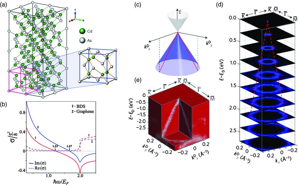
A thorough knowledge of the fundamental material properties of 3D DSM () has become critical for the right interpretation of a broad variety of observed and still unknown physical phenomena. has a rather complicated crystal structure [Fig. 1(a)] with a unit cell containing 160 atoms. According to the current consensus, is a tetragonal material with a unit cell of and at room and lower temperatures, which are the most important for basic and practical study of this material. The specific space group remains a point of contention. Recent research indicates that the centrosymmetric space group (No. 142)36,37 is preferable to the noncentrosymmetric space group (No. 110), as previously proposed.38 For a complete understanding of , assigning the correct space group is of critical importance. The spin degeneracy is lifted when space inversion symmetry is absent, which may result in the Dirac nodes splitting into pairs of Weyl nodes.36 A further point of interest is the fact that the crystal structure of , though clearly tetragonal, remains nearly cubic ().34 Thus, the lattice may be thought of as a collection of antifluorite (cubic) cells devoid of two cadmium cations [Fig. 1(a)]. A relatively big unit cell of is generated due to the cadmium vacancy ordering.
Additionally, it is necessary to emphasize that the crystal structure of experiences a series of polymorphic phase changes above ambient temperature. Each of these phase transitions is followed by a sharp shift in the crystal’s lattice constants, which may result in microcracks. Notably, regardless of the growth process, crystals of can only be formed at temperatures more than 425°C. The intricacy of the crystal lattice has a direct effect on both the physical characteristics of and our understanding of them. The electronic structure of was investigated by many groups using angle-resolved photoemission spectroscopy (ARPES).3,12,13,34 possesses a pair of 3D Dirac fermions near the msub point, with strong anisotropy between the and momentum directions detected through the analysis of the band dispersions along the , , and momentum directions. With a comprehensive map of the 3D Brillouin zone, it is feasible to find the Dirac points and examine their dispersions along all three momentum directions (, , and ). The cone shape dispersion along the and directions can be seen in Fig. 1(e), where the 3D plot of the ARPES spectra intensity clearly demonstrates linear dispersions along both directions with limited anisotropy. Figure 1(d) illustrates that the contour plots at different binding energies exhibit a cone-shaped dispersion that becomes ring-shaped at higher binding energies, evolving from a point (the Dirac point).
A random phase approximation theory (RPA) can be used to calculate the complex conductivity of the DSM.35 By incorporating the intraband and interband contributions to the dynamic conductivity of the DSM,35 one can develop the following equation: where with being the Fermi distribution function, is the Fermi level, is the Fermi momentum with equal to , , , ( is the cutoff frequency), and is the degeneracy factor. At low-temperature limit , the Eqs. (1) and (2) can be written as
In Eq. (4), the first term comes from the intraband conductivity and has a Drude-like form. On the other hand, the second logarithmic term represents the negative contribution of the interband transitions (the dielectric response). As demonstrated in Eq. (3), the real component of the 3D DSM conductivity is likewise derived from interband transitions and is responsible for optical absorption. Unlike graphene, which exhibits constant absorption, 3D DSM has a linear frequency absorption, as empirically demonstrated.39–41 It is evident from Eq. (4) that the imaginary part of 3D DSM conductivity differs from graphene due to its cutoff energy dependence. It should be noted, however, that in 3D DSM, the dielectric response is dominant at some frequencies. Further, in 3D DSM, the dielectric response may be observed at frequencies below because of the interband contributions from bands lower than the valence one that are not taken into account in Eqs. (3) and (4). Thus, in order to conduct an effective analysis of the dielectric response, one must investigate the dielectric function of 3D DSM in depth.
3 Fabrication Techniques
growing technology comprises a variety of techniques stretching back over fifty years. These provide a variety of sample morphologies, including bulk or needle-like crystals, thin films, microplatelets, and nanowires. In addition to mono-crystalline and poly-crystalline samples, there are also amorphous samples with varying qualities and doping levels. The high carrier density (from to ) of in bulk pushes the Fermi level further from the Dirac point.42 This high carrier density can be suppressed by reducing the dimensions of from bulk to thin films and nanostructures.43 In addition, displayed good optoelectronic capabilities and high energy conversion properties that rely largely and significantly on the synthesis methodologies.44 To achieve excellent device performance, the synthesized thin films and nanostructures must have excellent crystalline quality and unique morphologies. In recent years, there has been considerable interest in the development and characterization of . The thin films and nanostructures of can be synthesized by various methodologies, namely, physical vapor deposition (PVD),44 pulse laser deposition (PLD),45 molecular beam epitaxy (MBE),46 chemical vapor deposition (CVD),47 and self-selecting vapor growth (SSVG).34 In this section, a quick overview of the specifics of these synthesis procedures will be provided.
3.1 Molecular Beam Epitaxy
MBE is a robust deposition method for the development of high-quality, large-area epitaxial thin films. MBE is better than CVD and other deposition techniques due to its capacity to build heterostructures and superlattices with abrupt interfaces, as well as its chemical component versatility and fine control over film thickness. The ultrahigh vacuum (up to 10−10 mbar) in the MBE work chamber causes the formation of very pure thin films. In addition, several characterization techniques including ARPES and reflection high-energy electron diffraction (RHEED), can be coupled with MBE to in situ monitor the deposition process and electronic structure.48 Based on these outstanding features, MBE is a highly suitable deposition technique to grow thin films and their heterostructures. Liu et al.21 reported the first-ever growth of thin films by using the MBE technique and they demonstrated tunable properties like ambipolar effect and quantum oscillations in deposited wafer-scale films. The combined MBE and PLD technique was employed by Uchida et al.45 to achieve thin films with high-crystallinity and high-mobility. Schumann et al.49 used MBE to create highly crystalline epitaxial thin films. They discovered an expanded energy gap in bulk electronic states and, at low temperatures, the adequate mobility of carriers in surface states made it possible to investigate quantized Hall effects in MBE-grown thin films. Yang et al.46 fabricated thin film p–n heterojunction-based ultraviolet (UV) to long-wave infrared (LIR) photodetectors via MBE. The MBE grown heterostructures-based device showed excellent responsivity of , fast response time higher than , and a high on–off ratio of 6268. In LIR region, the responsivity and on–off ratios were and 100, respectively.46 As demonstrated in Fig. 2(c), these thin film photodetectors are very flexible. The findings revealed that thin film p–n heterojunction devices generated by MBE are highly desirable for high-speed and wide-band photodetectors.
PLD is a very advantageous process for depositing thin films of materials with high melting points, complicated stoichiometry, and sandwich architectures. In PLD the source material is bombarded with a high-energy focused pulsed laser and the small bombarded region converts into a plasma state. This bombarded pulse can raise the temperature of that microregion up to ten thousand degrees in no time. Since the high energy source is located outside the working chamber, PLD provides the flexibility of deposition in both ultrahigh vacuum (UHV) and inert gas environments. In UHV, the particles have eccess energy resulting in the deposition of nanocrystalline supersaturated solid solution and amorphous alloys. In the ambient inert gas environment, the energy of the particles can be controlled; consequently, the properties of deposited films can be tuned. The most important feature of PLD is to grow highly stoichiometric thin films of various kinds of materials ranging from metals to semiconductors and insulators. The thin film deposition rates of PLD are high as compared with other deposition techniques and multilayered structures can be grown easily.54,55 These attributes make PLD a highly desirable technique to grow thin films of 3D DSM . As illustrated in Fig. 2(d), Dubowski and colleagues51 used the PLD approach to develop stoichiometric polycrystalline on quartz substrates at ambient temperature, which was 140 K lower than the temperature necessary to create equivalent films via thermal evaporation. The carrier concentration and mobility of PLD grown films were reported to be and , respectively. To investigate the quantum transport phenomena in 3D DSM requires a high-quality film. Uchida et al.45 established a growth approach by combining PLD and solid phase epitaxy to generate high-quality single-crystalline films with controllable thickness, and they evaluated the influence of thickness on the quantum Hall effect. The quantum Hall states shown in high-quality films open the way for quantum transport and device application research in topological DSM.
3.3 Physical Vapor Deposition
PVD encompasses a wide range of thin film deposition and nanostructure fabrication processes, including evaporation, sputtering, laser ablation deposition, vacuum arc-based deposition, and several more. In PVD, the atoms or clusters of atoms of solid materials are typically removed by either thermal heating the source material or bombarding it with very energetic particles such as electrons, atoms, molecules, ions, or photons.48 In evaporation and ablation deposition, the removal process is thermodynamical. In sputtering, on the other hand, the removal of atoms from the source material is accomplished by a series of collisions with energetic particles at the material’s surface, a process known as the kinetic ejection of atoms. These ejected species pass through an evacuated chamber and strike the substrate, forming thin films.56 Li et al.44 have successfully synthesized extremely crystalline nanoplates and nano-octahedrons in a horizontal furnace using the PVD technique. Figure 2(a) depicts the nucleation and growth process of nanostructures. The fabricated nanostructures/metal electrode exhibited good photovoltaic performance for self-powered photo-detection applications.
3.4 Chemical Vapor Deposition
Among all other deposition techniques, CVD provides feasibility to synthesize both thin films and nanostructures for large-area synthesis. In CVD, thin films or nanostructures are formed on heating substrates by means of a chemical reaction of gaseous or vapor species. This process can involve a variety of gaseous, liquid, and solid chemicals as source material for the fabrication of thin films. As compared to other deposition techniques, CVD is more versatile, adaptable, compatible, simplest, reproducible, productive, and cost-effective.52,57,58 All of these characteristics make CVD the preferred method for synthesizing nanostructures with diversely controlled morphologies. Zhang et al.43 synthesized nanostructures with various morphologies, including nanowires, nanoribbons, nanobelts, nanoplates, and nano-octahedrons, using a simple CVD process. The schematic of the CVD growth mechanism of nanowires can be visualized by Fig. 2(b). All of these morphologies may be adjusted by altering the working chamber’s pressure and argon gas flow rate. Magnetoresistance investigation showed that CVD-grown nanostructures with diverse morphologies are advantageous for future nanoelectronic applications of DSM. Wu et al.52 fabricated graphene/ heterostructures [Fig. 2(e)] by CVD and observed a significant interlayer charge transfer that helped modify the Fermi level of graphene via . These heterostructures have potential spintronics uses. The CVD fabricated heterostructure-based photodetectors presented excellent performance with a high on–off ratio (), responsivity () at 520 nm, and an outstanding detectivity () at 808 nm in near infrared (IR) band.57
3.5 Self-Selecting Vapor Growth Technique
The self-selecting vapor growth (SSVG) method is a sealed tube method, suitable to grow single crystals of 3D DSM . The main distinctive advantage of this method is that the polycrystalline source material acts as a seed.59 In this method, the growth capsule remains static and transportation of vapors is carried out by a small temperature gradient. The key feature of this deposition method is that material evaporates from the hotter part source material and recondensed on the cooler part by itself.53 This process makes it possible to selectively generate crystal grains, resulting in the production of stress-free single crystals of increasing size and decreasing quantity.53,59 The little variation in temperature between the evaporation and deposition portions of the source material is another essential aspect of this approach. Due to this small temperature difference, the driving force for distillation-like separation is low, and crystals produced under these conditions exhibit minimal compositional separation.59 Sankar et al.53 reported the formation of huge plate-shaped single crystals of in an alumina furnace using the SSVG technique. Figure 2(f) is a cross-sectional view of the SSVG alumina furnace used for the creation of single crystal .
The experimental conditions including experimental methods, precursors/targets, substrates, and growth temperatures for the growth of thin films, nanostructures, and single crystals are briefly summarized in Table 1. In addition, the comparison of the advantages and disadvantages of various fabrication techniques is tabulated in Table 2.
Material
Preparation method
Precursor/target
Growth temperature
Substrate
Reference
thin film
PLD
Mixture of 6N5 Cd and 7N5 As shots target
Room temperature
Ref. 45
thin film
PLD
Single crystal target
Room temperature
Fused quartz plates
Ref. 51
nanostructures
PVD
powder
650°C
Ref. 44
thin film
MBE
bulk
170°C
Mica
Ref. 21
thin film
MBE
target
140°C
CdTe
Ref. 60
thin film
MBE
target
150°C to 170°C
GaAs
Ref. 49
thin film
MBE
target
180°C
GaAs (111)B
Ref. 61
nanostructures
CVD/ vapor solid mechanism
powder
760°C
Si
Ref. 47
nano-belts
CVD
powder
760°C
Quartz
Ref. 52
microbelts
CVD
powder
760°C
Si
Ref. 58
submicron wires
CVD
powder (6N pure)
Upstream: 650°C Downstream: 350°C
coated with L / ethanol solution
Ref. 62
single crystals
CVD
Cd and As powders
825°C
—
Ref. 63
single crystals
SSVG
Stoichiometric mixture of Cd and As elements
850°C
—
Ref. 53
Table 1. Growth conditions for thin films, nanostructures, and single crystals for various growth techniques.
Optical harmonic generation (OHG) is a nonlinear phenomenon that is utilized to investigate low-dimensional physics.68 It is employed in the field of bioimaging, optical signal processing, and the development of innovative coherent light sources.69 The study of these interactions is the heart of nonlinear optics, and a cornerstone of modern photonics. In particular, the extreme sensitivity of OHG to material characteristics, crystallinity, and defects, as well as its dependency on excitation parameters, permits a diverse array of applications and nonlinear optical devices.70–73 Conventional nonlinear devices are comprised of bulk materials such as beta barium borate (BBO), potassium titanyl phosphate (KTP), or lithium niobate ().70 On-chip integration and multifunctional or tunable devices are not feasible with these materials.74,75 Plasmonic materials have been presented as nonlinear materials due to their ability to significantly increase nonlinear processes by restricting the field to a nanometric area.76–79 Due to their significant dissipative losses, they are not suitable for nonlinear materials.80 High-index dielectric nanomaterials have been introduced as a favorable alternative because of their strong magnetic response and low losses.81,82 Despite these advancements, the effectiveness of nonlinear effects in these metasurfaces or nanostructures still falls short of the requirements of current nonlinear devices.74 After discovering graphene in 2004,83 much effort has been made to uncover the nonlinear physics in other 2D materials beyond graphene.70,71,73,84 The enormous nonlinear coefficients of these atomically thin materials may allow them to replace conventional nonlinear media in photonic systems. A comparison of different materials in producing OHG is provided in Table 2. We are well aware that an exact comparison of requires consideration of a number of elements, including the working wavelength, manufacturing technique, substrate, and thickness. Each of these factors has a substantial influence on the . We have used a typical value of to get an approximate estimate of . Due to the fact that graphene and (3D equivalent of graphene) are centrosymmetric, only values are considered in Table 3.
Nonlinear material
Reference
/
Phase control
Advantage
Disadvantage
Traditional bulk material ()
Refs. 85, 86
No
Commercially available
Weak nonlinearity
Plasmonic nanostructures (gold)
Refs. 86–88
Yes
Strong field enhancement
High losses
Dielectric nanostructures
Refs. 89 and 90
Yes
Low losses
Moderate field enhancement
2D materials thin films
Refs. 69, 91, 92
Yes
1. Tunable
1. Due to atomic thickness the light–matter interaction is weak.
2. Easily integrated with other bulk structures
2. Making nanostructures is difficult
thin film
Ref. 93
Yes
1. Tunable
Need to be explored (Very few experimental findings and minimal understanding)
2. Extendable to other structures
3. Easy to make nanostructures
Table 3. Comparison between nonlinear efficiency with other materials including advantages and disadvantages.
In 2020, terahertz-field-driven high-harmonic generation (HHG) in was demonstrated experimentally at ambient temperature.32 The third-, fifth-, and seventh-order harmonic generation were extremely efficient when excited by linearly polarized multicycle terahertz pulses and identified using time-resolved spectroscopic methods, as provided in Fig. 3(b). Further investigation of the reported harmonic radiation is performed as a function of pump-pulse fluence. In the perturbative regime, their fluence dependency deviates significantly from the anticipated power-law dependence. Similarly, one more group observed a significant THz HHG in thin films of at ambient temperature.95 It was demonstrated that third harmonic generation (THG) can be detectable using a tabletop light source and can be as strong as when a fundamental field of is applied within the film, exhibiting an exceptional efficiency for terahertz frequency conversion. In the same year, Ullah et al.93 performed the THG investigation in thin films. They measured THG in two types of fabricated devices at telecommunication wavelengths. In one device, is fabricated on a mica substrate, while in the other, a micro planar cavity is embedded underneath the . They discovered a significant increase in the THG signal of up to 420 times in the device with a planar cavity compared with the device with bare thin film on a mica substrate. On comparing the THG signal and of , glass, , and graphene under the same measurement conditions [Fig. 3(d)], it was determined that the has a value of , which is 1000 times more than the value of glass and 1.3 and 1.5 times greater than the values of and graphene, respectively. Theoretically, the creation of HHG in 3D DSM via THz radiation has also been investigated recently.33,94 It was demonstrated that 3D DSM is a promising solid-state platform for the highly efficient generation of extreme intraband-dominated THz harmonics up to the 31st order [Fig. 3(c)] and beyond using input field intensities of —a factor of reduction in intensity over previous THz HHG demonstrations.94 According to another study,33 when a film thickness of 50 nm is increased to 1500 nm, the output intensities of the 3rd and 31st harmonics may be increased by factors of 144 and 28, respectively. More intriguingly, it was shown that highly nonlinear materials like 3D DSMs enable the appearance of a subwavelength phase-flip in the induced current density at nanoscale propagation lengths. This effect has not been seen in nonlinear materials that are typically used. There are a few additional theoretical publications96,97 that explain the OHG in 3D DSM, including the second harmonic generation (SHG) in tilted DSMs with a broken tilt inversion symmetry when no external magnetic field is present.97
Recent advances in DSMs have focused attention on the strong coupling of electromagnetic radiation in these materials through plasmons. This enables subwavelength confinement and intense light–matter interaction, which is advantageous in a wide variety of nanophotonics applications.98,99 There are two distinct characteristics of these plasmons. First, unlike parabolic band materials, these plasma oscillations are predominantly quantum mechanical in nature (since is regarded as the leading term of the plasma dispersion relation). Additionally, these charge oscillations disappear when the Fermi level reaches the Dirac point ().100 The second reason is that, in contrast to parabolic band materials, the linear energy dispersion in DSMs leads to a lower-order dependency of the plasmon resonance frequency () on charge density (), implying that plasmon resonances occur mostly at terahertz frequencies.101 The existence of significant terahertz coupling in these materials, together with their ease of tuning and lengthy momentum scattering time (), has been envisioned to play a crucial role in the emerging area of terahertz electronics and optoelectronics. Up to the present, research efforts in this area have been primarily motivated by investigations of plasmons in 2D DSM graphene.102 Interestingly, the recent experimental demonstration of long expected 3D counterparts of graphene3,12–15 inspires additional research on electromagnetic phenomena and light–matter interaction, such as Dirac plasmons. In this aspect, the 3D character of 3D DSMs distinguishes them from their more often researched 2D counterparts.
Current theoretical research on plasmons in 3D DSMs reveals a fundamental difference in their dispersion relations when compared with 2D DSMs. The plasma frequency () dependence in 3D DSM is 103,104 whereas it results in in the case of 2D DSM.101,102 The larger Fermi velocity in 3D DSM is very advantageous for creating plasmon resonances with a higher quality factor ().101 This is comparable to the situation in parabolic band materials, where low effective masses and lengthy momentum scattering periods are linked with high quality factors in plasmonic resonances. The authors of a recent study100 demonstrated that patterned resonant plasmonic devices have spectrally narrow terahertz plasmon resonances [Fig. 4(a)]. This finding was ascribed to the extremely long momentum scattering time seen in films, which is a direct result of the enormous defining the Dirac dispersion. Ooi et al.19 reported that 3D DSM had the comparable nonlinear plasmonic performance to graphene while keeping the structural advantages of bulk metals, minimizing passive plasmonic losses, and being far simpler to handle in fabrication facilities. The surface plasmon propagation lengths of were found to vary by up to three orders of magnitude between the bulk and thin film forms [Fig. 4(b)]. The same is true for bulk gold and thin gold films, whereas graphene, with a thickness of an atomic layer, has the same surface plasmon propagation lengths as thin films. Tunable propagation characteristics of 3D DSM-based hybrid plasmonic waveguides were explored.106 The proposed hybrid waveguides exhibit strong (weak) confinement when the operating frequency is less (greater) than the transition frequency, due to the DSM layer’s high plasmonic (dielectric low) loss feature. Similar plasmonic investigations in 3D DSM-based hybrid structures were investigated107,108 in order to enhance the understanding of this topic.
Similarly, it was numerically demonstrated that 3D DSM is a flexible option for demonstrating the TE plasmonic mode.109–113 The TE plasmon mode is often weakly limited and very difficult to see experimentally due to its sensitivity to the permittivity difference between adjacent materials.114 The use of innovative low-dimensional materials, periodic multilayer structures, nonlinear materials, etc., helped to increase the TE plasmonic mode confinement and enable experimental observations.115–118 For example, the spatial confinement of the TE plasmon was considerably increased by the 2D hexagonal boron nitrides layer, which was also very stable and existed even when the superstrate and substrate had a highly different permittivity.116 With a graphene-metamaterials hybrid structure, the TE plasmon contributed significantly to the heat exchange and was effectively used to explore near-field radiative heat transfer.117 The 3D DSM layer has a substantially greater thickness than graphene, making the TE plasmonic mode stronger and easier to create from an experimental standpoint. To investigate high-efficiency mid-IR spectral devices, a 3D DSM TE plasmonic structure has been investigated systemically, revealing that the obvious TE mode can be achieved when the Fermi level is not very large and the temperature is relatively high (about 100 K), in contrast to the graphene symmetric structure, which must operate at low liquid helium temperatures.3,110,113,119–121 It was discovered that when the Fermi level rises, the transition frequency of TE modes increases and the peak location of the real and imaginary portions of effective indices exhibit evident blue shifts. At low temperatures, the interband transition contributes more, and the 3D DSM layer exhibits improved dielectric characteristics and enables a stronger TE mode.122
Plasmon-induced transparency (PIT) is a plasmon analogue of electromagnetically induced transparency. It is created by significant destructive interference between plasmon super-radiation and plasmon subradiation modes.123,124 Its remarkable dispersion properties and wide range of uses have attracted researchers’ curiosity. Recently, researchers presented a range of devices capable of producing the PIT effect. For instance, plasmonic waveguide coupled resonators, metamaterials, and metasurface structures have all been shown.125–127 The majority of these devices are made of metallic materials, and it is almost hard to control the material’s dielectric function and loss. Due to the metal’s limited surface plasmons, modulation performance is exceedingly low. A dynamically tunable PIT effect is needed in real applications. Once constructed, the shape of the device is impossible to modify, and its singularity precludes practical usage. Additionally, few studies have been conducted on the tunable PIT effect. As previously mentioned, similar to graphene, the optical conductivity of 3D DSM may be tuned easily due to its structure. As a result, researchers produced a highly controllable PIT effect in metamaterials based on 3D DSM.105,128 Chen et al.129 also explored the multiband PIT effect. Additionally, a metamaterial based on 3D DSM was also reported that was very wide and tunable.130 Certain researchers presented a waveguide structure device for implementing the PIT effect that is simpler to incorporate into an optical circuit than the metamaterials-based 3D DSM.131
4.3 Ultrafast Photocarrier Dynamics in
Generally, the ultrafast dynamics of a material referred to its response to the excitation of an optical pulse (either pump or probe) with a timescale of sub- and pico-seconds (ps). Both pulse types have a typical duration of 20 to 100 femtoseconds (fs).132 When the sample comes into contact with the pump, its characteristics are momentarily altered, mostly via the excitation of electrons and phonons and the changing of the electronic band structure. It is possible to monitor the changes with a probe pulse that is delivered at a variable time after the pump: for example, by measuring the reflectivity, transmissivity, or photoelectron spectrum. Ultrafast experiments are set to play a critical role in the research and use of topological materials, most notably the 3D DSM.133 The majority of the features of 3D DSM, including their linear band dispersion, Berry curvature, the near-vanishing density of states at Fermi energy, and sensitivity to crystalline and time-reversal symmetry, are intimately tied to their sub- and few-picosecond reaction to light.132 The ultrafast responses of numerous DSMs have been measured and are now in practical use. These materials were utilized to create a passive optical switch for picosecond mode-locking of a midinfrared laser134 and broadband infrared photodetectors46,135 with response times of a few picoseconds.
Weber et al.136 determined the ultrafast transient grating properties of at both room temperature and 80 K in 2015. Following photoexcitation with 1.5-eV photons, charge carriers undergo two relaxation processes, one lasting 500 fs and the other lasting 3.1 ps. The authors determined that by measuring the complex phase of the change in reflectance, the faster signal corresponds to a reduction in absorption and the slower signal to a drop in the phase velocity of light at the probe energy. The hot-carrier relaxation dynamics in thin films was investigated by Zhu et al.137 The combination of degenerate and nondegenerate pump-probe spectroscopy revealed that the hot carrier distribution in is formed on a period of about 400 fs. Numerous studies on the dynamics of photocarriers in were conducted utilizing ultrafast optical pump and optical probe spectroscopy in the visible and near-to-midinfrared regions.17,134,137,138 Zhang et al.113 used terahertz spectroscopy to study the ultrafast photocarrier dynamics in a thin film as can be visualized in Fig. 5(b). THz radiations have a very low photon energy, and optical pump and THz probe (OPTP) spectroscopy can be utilized to study photocarrier dynamics at the Fermi surface.139 Time-resolved THz spectroscopy is a noncontact and noninvasive spectroscopy technique that enables the analysis of material’s high-frequency photoconductive response on subpicosecond time scales. By evaluating the real and imaginary components of the complex conductivity spectrum, it is feasible to derive the development of both the concentration and mobility of charge carriers with ultrafast temporal precision. It was discovered113 that using an optical pump may result in significant absorption in the thin film at THz frequencies. Following photoexcitation, the maximal THz photoconductivity is obtained with a time constant of 1.0 ps that rises slightly with pump fluence, and the following decay proceeds by a single exponential relaxation with a typical lifespan of 6.0 ps, regardless of pump fluence. Another time-resolved terahertz spectroscopic study23 in a thin film at room temperature revealed a modulation depth of 63% at a record low optical fluence of with an ultrafast switching time of 15.5 ps [Fig. 5(c)]. Several other studies132,138,139 on photoexcitation dynamics in were carried out by different researchers in order to enhance the understanding of this topic. Additional knowledge of the 3D DSM photoexcitation response will be crucial for basic research, including establishing a predicted exciton condensate, linking photocurrents to electronic topology, closing or opening gaps at Dirac points, and converting nodal lines to point nodes.
Absorption enhancement is a critical component of optical devices and has garnered much attention in recent years. Theoretically, a perfect absorber is created by limiting reflection and eliminating transmission. Since Landy et al.140 first reported a flawless metamaterial-based absorber in 2008, metamaterial-based absorbers have been intensively explored and proven across a wide variety of spectral ranges, including microwave,141 terahertz,142 and infrared.143 Their popularity stems from their versatility in a variety of applications, including thermo-photovoltaics,76 sensors,144–146 and filters,147,148 as well as thermal radiation tailoring.149,150 For the most part, an absorber is made up of a metal-dielectric-metal (MDM) structure, with the metal layer on top serving as an impedance matcher and the metal layer below serving as a transmission-blocking “salisbury screen,” however, if the metal layer below is too thin, the MDM arrangement may be utilized as an optical device to boost transmission.151 Due to radiative damping and nonradiative losses, these absorbers have very large absorption bandwidths, which is advantageous for a broadband absorber. Fortunately, nonradiative losses may be decreased by replacing the upper metal layer with a low-loss material, such as a dielectric.152,153 Unfortunately, ideal absorbers based on conventional noble metals such as gold, silver, or copper are constructed with fixed absorption peaks and must have their geometric parameters meticulously reoptimized if the absorption peaks have to be tuned to different frequency regions.154
2D materials have been employed to improve the absorber’s stability and absorption. Graphene is one of the most widely used 2D materials and has shown great promise in metasurface applications.155 Graphene’s optical response is defined by its surface conductivity, which is related to its Fermi energy and may be modified dynamically using a bias voltage.69 Various researchers have successfully achieved dynamically tunable perfect absorption using 3D DSM. For example, Liu et al.156 suggested a narrowband absorber in 2018 that made use of the metallic feature of 3D DSM at THz frequencies and achieved a total quality factor of 94.6.36 Similarly, when the Fermi level is between 65 and 85 meV and the resonance frequency is between 2.46 and 3.16 THz, tunable narrow band absorbers with absorption have been obtained. Dai et al.157 developed a broadband terahertz cross-polarization conversion based on 3D DSMs that can be controlled by adjusting the Fermi level of the 3D DSMs, with the polarization conversion rate typically exceeding 80%. Several other proposed designs of 3D DSM absorbers have been proposed including the ultrahigh tunable 3D DSM absorber158 and triple band absorber159 based on 3D DSM. These proposed designs for a 3D DSM absorber open new avenues for the construction of tunable absorbers and may have applications in photovoltaic technology.
4.5 Some Other Photonics of
Enhancing our knowledge of photonic modes in nanomaterials enables us to better understand the underlying processes involved in optoelectronic devices and optimize their performance. Surface waves have drawn considerable attention as types of photonic modes, including surface plasmon polaritons (SPPs) and quasicylindrical waves (QCWs).160–163 The QCW is an optical field scattered by subwavelength indentations, distributed along a surface over several wavelengths, containing both radiative and evanescent components. The optical QCW on nanoplates has recently been studied164 by a team of researchers across a wide range of wavelengths from ultraviolet (UV) to visible. It was found that QCW is of the same wavelength as the input light and decays at a rate of from the scattering source. Transverse magnetic modes were found to dominate the QCW pattern, depending on the excitation polarization relative to the nanoplate edges.164 Additionally, numerical simulations indicated that the metasurface may improve absorption when compared with naked nanoplates. This is advantageous with the aid of QCW, since the interference between the incoming light and QCW modes results in a stronger local field, which increases absorption.
In a recent paper,16 the authors investigated the thermo-optic characteristics of epitaxially grown using infrared spectroscopy and demonstrated significant optical tunability in the mid- and far-infrared regions [Fig. 6(d)]. The finding is significant since many of tunable optical and thermal characteristics remain unknown. Furthermore, understanding the dynamics of charge carriers perturbed by electromagnetic fields is critical for understanding the underlying physics of optical excitations. It was proved that tuning the Fermi distributions results in a substantial infrared thermo-optic shift. The results described in this article may stimulate more studies into the tunable optical and electrical properties of Dirac and Weyl semimetals and may pave the way for novel applications in reconfigurable optoelectronic and nanoscale thermal devices.16
The coding metasurface idea entails the creation of arrays of coding unit cells having a phase response from 0 to .166 Then, by optimizing the coding sequence of the microstructures, the suggested metasurfaces may be utilized to flexibly alter electromagnetic waves.167 For instance, two adjacent units with a phase difference of 180 deg correspond to two elements (‘0’ and ‘1’ elements) of a one-bit coding hypersurface.168 Recently, graphene was introduced for the purpose of fabricating tunable coding metasurfaces.169,170 However, graphene’s structure is very thin and is quickly altered by its dielectric surroundings. Additionally, fabricating graphene-based metasurfaces is challenging. In order to solve these issues, a switchable coding metasurface was developed to enable dynamic beam steering based on a 3D DSM in the THz frequency range.165 It was shown that the suggested metamaterials unit cell’s relative phase delay may be actively controlled by altering the Fermi level () of the 3D DSM. By varying the value of the 3D DSM for the 1-bit coding metasurface, the coding units with “0” and “1” states may be turned on/off in the frequency range from 1.46 to 2 THz. In such 1-bit coding metasurfaces, the beam numbers and propagation direction of the reflected waves may be programmed arbitrarily. Additionally, a dynamically controlled two-bit coding metasurface based on 3D DSM microstructures was built into the work to enable more advanced beam modulation.
In response to the question of whether 3D DSMs have an intrinsic topological signature that can be seen in the optical spectrum, the answer may be connected to chiral anomalies, which is one of the distinguishing properties of these systems.171 Optically, minimal experimental data, such as a significant Kerr rotation in ,172 has been demonstrated, although several theoretical approaches have been proposed about this feature. For observable experimental characteristics, however, low temperature and good quality samples are recommended, since high temperature and scattering processes induced by contaminants may smooth out these features.
5 Applications of Photonics of 3D DSM
Since the beginning of the 1990s, semiconductor saturable absorber mirrors (SESAMs) in the early 1990s have been a crucial technique in the near-infrared sector.20 SESAM is one of the most essential saturable absorber technologies because of its adaptability and precision. It can be included in numerous laser formats, such as fiber, solid-state, and semiconductor chip lasers.173–175 By monitoring the midinfrared optical response of the bulk Dirac fermions, it has been shown that MBE-grown thin films may function as an efficient ultrafast () optical switch in the midinfrared, with a working range spanning at least from 3 to .20
Ultrafast response time, broad wavelength range, and great sensitivity make photodetection ideal for optical communications, optical interconnects, imaging, and remote sensing, among other optoelectronic and photonic applications.17 An outstanding photodetector based on graphene has demonstrated tremendous promise for fast operating speeds, broadband responsiveness, and efficient carrier multiplications, all of which benefit from its linear dispersion band structure with high carrier mobility and zero bandgap. As the 3D equivalent of graphene, DSM has all of graphene’s benefits as a photosensitive material but can interact with light more strongly as a bulk material, resulting in increased reactivity. Various 2D materials-based photodetectors can significantly suppress dark current and the efficient photon absorption from the visible to near-IR region, resulting in an enormously enhanced photoresponse. Due to their nearly gapless band structure, topological materials are able to achieve low-energy photon absorption; as a result, photodetectors based on these materials have an enormous advantage in terms of detection range, up to the far-infrared and terahertz range.20 Among all other topological semimetals, is easy to synthesize and is highly stable in air atmosphere.93 The simple development of thin film and its compatibility with other semiconducting materials make it suitable for use in infrared cameras and wide-band photodetection.176 On the other hand, its nearly zero bandgap gives rise to a larger dark current and adversely affects the responsivity of the device. To suppress the dark current and improve the responsivity, the heterostructure of with other materials can be formed. The rectification effect of the heterostructure and the effective charge carrier separation lead to suppress the dark current and hence improved responsivity of photodetector.176 In this work,17 the development of a -based ultrafast broadband photodetector was discussed. Without any device optimization, the prototype metal--metal photodetector exhibited a responsivity of and a response time of around 6.8 ps. It was possible to generate broadband responses from 532 nm to 10.6 m, with a potential detection range extending to far infrared and terahertz. However, the high conductivity of prototype metal--metal photoelectric devices generates a substantial dark current, which significantly limits the enhancement of performance characteristics such as responsivity and detectivity. To overcome this limitation and enhancing the parameters of photoelectric devices, heterostructure-based fast photodetection devices have emerging applications in modern optoelectronic industry.176 In comparison to the metal--metal device, the (copper-phthalocyanine) heterostructure based photodetector recently shown superior figure of merit.177 Under irradiation of 808 nm, the heterostructure-based device showed optimal values of performance parameters including detectivity () and responsivity () that are much enhanced as compared with the detectivity () and responsivity () of pure metal--metal device.177
Due to its high carrier mobility and variable carrier concentration, provides an attractive possibility for high performance applications, such as plasmonics and optoelectronic devices based on 3D DSM plasmons.19 In contrast to noble metal plasmons, 3D DSM plasmons19,178 are broadband and display exceptionally strong confinement, enabling light-matter interaction for quantum optics, chemical identification, and biosensors.20 Importantly, the tune-able surface conductivity expands the application potential of . There are various photonic uses of such as tunable absorber157,158 and polarizer,157 that make it a perfect choice in tunable photonic systems. Figure 7 depicts a schematic illustration of the use of the photonics of 3D DSM .
Figure 7.Schematic shows the potential applications that can generate with the photonics of 3D DSM .
We have discussed most recent developments in numerous photonic aspects related to 3D DSM , and in particular, cutting-edge photonic technologies based on 3D DSM such as linear and nonlinear plasmonics, optical absorption, optical harmonic generation, ultrafast dynamics, and several others. In addition, we have included a short review of current developments in synthesis methodologies. Reviewing its optical characteristics revealed that is a notable member of the topological materials class, which has been extensively investigated using both theory and experiment. There is no question that contains well-defined 3D massless charge carriers.
Without a doubt, 3D DSM will continue to draw the interest and effort of researchers. However, the synthesis of large-area, high-quality materials is always necessary not just for the demonstration of intriguing topological physics, but also for mass-scale device applications. In order to go ahead, methods of measuring and controlling must be devised. In reality, the creation of probes is necessary to fully understand many unusual quantum states. It may be necessary to use a variety of strategies under extreme conditions to make the most of these tools. Quantum control of the physics is another route that may be attainable via the integration of electrical and optical methods, resulting in practical applications. In particular, it is necessary to create approaches at various frequencies, particularly in the GHz and THz ranges, that are tuned to the fascinating topological quantum physics. Since the heterojunction179 device may increase the responsivity and external quantum efficiency in a wide range from visible light to far-infrared light, it is viable to employ heterostructures of and organic molecules to create photodetectors. Along this path, we anticipate achieving devices with greater responsiveness and external quantum efficiency using various organic compounds, as well as significantly expanding the responsive range (toward THz). In addition, it seems that the effort to use as a saturable absorber in the area of pulsed lasers is effective. is a highly adaptable near-infrared SESAM as a result of its primary properties, which include wide scalability, broadband functioning, and variable parameter control. We foresee the development of the suggested electrically contacted saturable absorber device. It may be extended further to active photonic devices working in the near-to-far-infrared spectrum, such as optical modulators and tunable light-emitting devices. In contrast to 2D semiconductors, which have been widely investigated, large-area 3D DSM fabrication experience is currently scarce. A general way to generate high-quality, wafer-scale films at a cheap cost and with a high yield has not yet been established, even though numerous fabrication processes have been reported.48
heterostructure-based photodetectors exhibit stronger and broadband photo-responsivity from the UV to far-IR regions. The IR imaging of is an extremely important step to raise the research level of 3D DSM for practical applications. In the future, more heterostructures can be designed to improve the responsivity and provide more solid foundations for its applications. Reduction in the carrier concentration of electrons in can enhance the lifetime of photo-generated carriers and allows more to reach the interface. To identify the ways to reduce electron concentration in as-grown highly n-type will be an important step. Utilization of transparent electrodes can improve the collection of photogenerated carriers, enhancing the number of photons reaching the junction.176 Progress in the growth of large area with high quality and integrability will improve over the coming years and will significantly improve the key device characteristics such as responsivity and detectivity.48 This will provide a pathway for to become an essential part of viable optoelectronic devices. Clearly, the investigation of the optical properties possessed by 3D DSM is still in its infancy, and we may be on the verge of discovering something a great deal stranger than what we had envisioned.
Renlong Zhou received his BS degree from Hunan University of Science and Technology (HNUST) in 1998, his MS degree from Hunan University (HNU) in 2003, and his PhD from Shanghai Institute of Technical Physics (SITP) of the Chinese Academy of Sciences (CAS) in 2007. Currently, he is a professor at the School of Physics and Information Engineering, Guangdong University of Education, Guangzhou, China. He directs the Research Institute of Terahertz Functional Devices. His research interests include photonic crystals, two-dimensional materials, light–matter interaction, nonlinear optics, surface plasmon, and applications.
Kaleem Ullah received his PhD in optical engineering from Nanjing University of Science and Technology (NJUST), China, in 2018. After that, he completed his postdoctoral fellowship at Nanjing University, China. Currently, he is a postdoctoral researcher at the University of Delaware, United States. His research interests include far-field super resolution microscopy, nanophotonics of dielectric nanostructures, plasmonics, integrated photonics, and light–matter interaction in two-dimensional materials.
Naveed Hussain received his master’s degree in physics from International Islamic University, Islamabad, Pakistan, in 2012, and his PhD from the School of Materials, Tsinghua university, Beijing, China, in 2019. Currently, he is working as a senior postdoctoral researcher at the School of Electrical and Computer Engineering, University of California Irvine. His research focuses on high-pressure syntheses and crystallographic engineering of ultrathin two-dimensiona materials, probed by using light–matter interactions at the nanoscale.
Mohammed M. Fadhali received his BSc degree from the University of Technology, Iraq, in 1997, his MSc degree from Cochin University of Science and Technology, India, in 2003, and his PhD from Universiti Teknologi Malaysia, in 2008. Currently, he is an associate professor of laser physics/photonics at Physics Department, Jazan University, Saudi Arabia. His research interests include ultrafast optical process, laser spectroscopy, plasmonic, and nanophotonic.
Sa Yang received her BE degree from Chengdu University of Information Technology (CUIT) in 1992 and her ME degree from South China University of Technology (SCUT) in 2007. He is an associate professor at the School of Physics and Information Engineering, Guangdong University of Education, Guangzhou, China. She is the dean of the School of Physical and Information Engineering. Her research interests include optoelectronic device design, micro/nano material characteristic analysis, and image information processing.
Qiawu Lin received his BS degree from Guangdong University of Education, China, in 2003, and his MS degree from Sun Yat-sen University, China, in 2010. Currently, he is pursuing a PhD at South China Normal University, China. Currently, he is an associate professor in the Department of Physics and Information Engineering, Guangdong University of Education, Guangzhou, China. He is the assistant dean of the Department of Physics and Information Engineering. His research interests include photonic crystals, two-dimensional materials, nonlinear optics, surface plasmon, and applications.
Muhammad Zubair received his PhD from Beijing University of Technology, China, in 2020. Currently, he is working as a research scientist in the Forschungszentrum Jülich, and will focus on the development of cathodes and electrolytes of solid-state lithium metal batteries. His research interests lie in synthesis and characterization of cathode materials for batteries.
Muhammad Faisal Iqbal received his PhD in physics from the University of Science and Technology of China, Hefei, China, in 2020. Currently, he is working as an assistant professor in the Department of Physics, Riphah International University Faisalabad, Pakistan. His current research interests are mainly focused on Raman spectroscopy, surface-enhanced Raman spectroscopy, and optoelectronic properties of semiconductor thin films and nanostructures.
Renlong Zhou, Kaleem Ullah, Naveed Hussain, Mohammed M. Fadhali, Sa Yang, Qiawu Lin, Muhammad Zubair, Muhammad Faisal Iqbal, "Recent advances in photonics of three-dimensional Dirac semimetal Cd3As2," Adv. Photon. Nexus 1, 024001 (2022)