• Laser & Optoelectronics Progress
  • Vol. 57, Issue 11, 111421 (2020)
Wen Gao1、2, Meiling Zheng1、*, Feng Jin1, Xianzi Dong1, and Jie Liu1
Author Affiliations
  • 1Key Laboratory of Bio-Inspired Materials and Interfacial Science, Technical Institute of Physics and Chemistry, Chinese Academy of Sciences, Beijing 100190, China
  • 2University of Chinese Academy of Sciences, Beijing 101407, China
  • show less
    DOI: 10.3788/LOP57.111421 Cite this Article Set citation alerts
    Wen Gao, Meiling Zheng, Feng Jin, Xianzi Dong, Jie Liu. Fast Fabrication of Large-Area Two-Dimensional Micro/Nanostructure by Femtosecond Laser[J]. Laser & Optoelectronics Progress, 2020, 57(11): 111421 Copy Citation Text show less
    Diagram of fabrication of polymer micro/nanostructure with positive photoresist
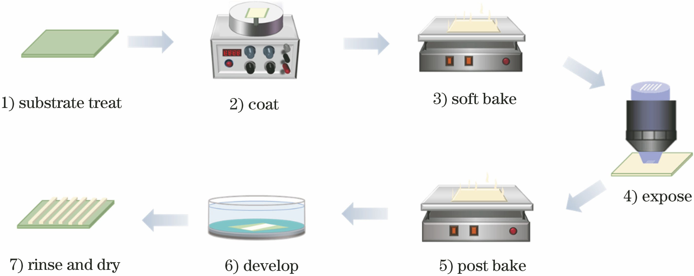
    Fig. 1. Diagram of fabrication of polymer micro/nanostructure with positive photoresist
    Experimental results of DMD based maskless lithography exposure. (a) Scanning electron microscope (SEM) image of 10 μm equidistant line array structure; (b) SEM image of 1 μm equidistant line array structure; (c) minimum line width of 250 nm; (d) line width versus exposure time
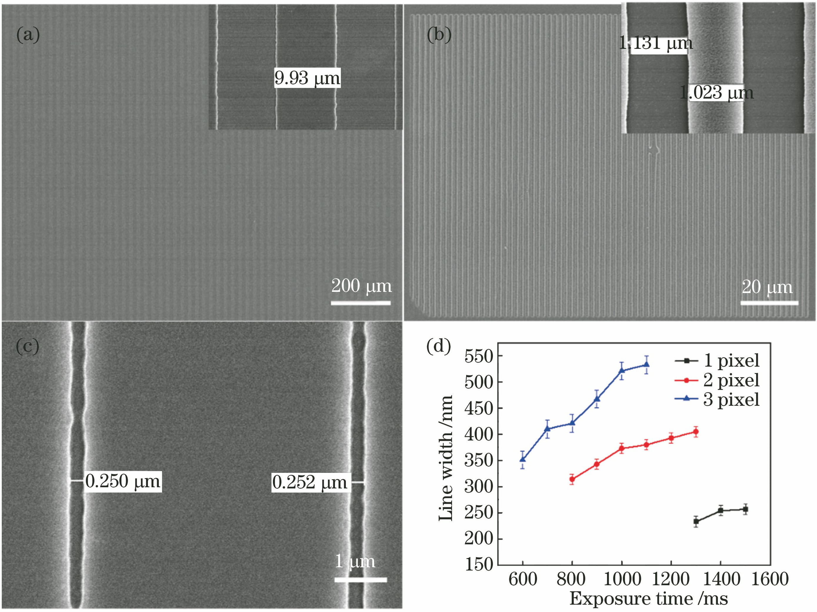
    Fig. 2. Experimental results of DMD based maskless lithography exposure. (a) Scanning electron microscope (SEM) image of 10 μm equidistant line array structure; (b) SEM image of 1 μm equidistant line array structure; (c) minimum line width of 250 nm; (d) line width versus exposure time
    Diagram of single optical field line scanning and results obtained. (a) Diagram of single optical field line scanning;(b) SEM image of 1 μm equidistant line array structure; (c) SEM image of 500 nm equidistant line array structure
    Fig. 3. Diagram of single optical field line scanning and results obtained. (a) Diagram of single optical field line scanning;(b) SEM image of 1 μm equidistant line array structure; (c) SEM image of 500 nm equidistant line array structure
    Characterization of width of trench structures fabricated by single optical field exposure and line scanning using atomic force microscopy. (a) (b) Topography of 1 μm equidistant line array structure fabricated by single optical field exposure; (c) height distribution of 1 μm equidistant line array structure fabricated by single optical field exposure; (d)(e) topography of 1 μm equidistant line array structure fabricated by single optical field line scanning; (f) height distribution of 1 μm equi
    Fig. 4. Characterization of width of trench structures fabricated by single optical field exposure and line scanning using atomic force microscopy. (a) (b) Topography of 1 μm equidistant line array structure fabricated by single optical field exposure; (c) height distribution of 1 μm equidistant line array structure fabricated by single optical field exposure; (d)(e) topography of 1 μm equidistant line array structure fabricated by single optical field line scanning; (f) height distribution of 1 μm equi
    Variation in trench width of 1 μm equidistant line array structures fabricated by single optical field exposure and single optical field line scanning
    Fig. 5. Variation in trench width of 1 μm equidistant line array structures fabricated by single optical field exposure and single optical field line scanning
    Diagrams of splicing and equidistant line array structures. (a) Diagram of complete structure; (b) diagram of partial structure; (c) SEM image of 1 μm equidistant line array structure; (d) SEM image of 10 μm equidistant line array structure
    Fig. 6. Diagrams of splicing and equidistant line array structures. (a) Diagram of complete structure; (b) diagram of partial structure; (c) SEM image of 1 μm equidistant line array structure; (d) SEM image of 10 μm equidistant line array structure
    Contact angle between equidistant line array structure and water drop, and contact angle between photoresist film and glass substrate. Variation in contact angle between 1 μL water drop and (a) 1 μm, (b) 3 μm, and (c) 5 μm equidistant line array structures in parallel and vertical directions relative to structure; (d) contact angle between photoresist film and glass substrate
    Fig. 7. Contact angle between equidistant line array structure and water drop, and contact angle between photoresist film and glass substrate. Variation in contact angle between 1 μL water drop and (a) 1 μm, (b) 3 μm, and (c) 5 μm equidistant line array structures in parallel and vertical directions relative to structure; (d) contact angle between photoresist film and glass substrate
    Contact angle varies with line space in parallel and vertical directions relative to structure
    Fig. 8. Contact angle varies with line space in parallel and vertical directions relative to structure
    Processing methodWidth of trench /μmVariance
    Single optical field exposure0.2820.2380.2270.2320.2540.2430.1990.1270.043
    Single optical field line scanning0.5400.5400.5200.5000.4800.5000.4800.5200.020
    Table 1. Widths of trench structures fabricated by two processing methods and variance analysis
    Wen Gao, Meiling Zheng, Feng Jin, Xianzi Dong, Jie Liu. Fast Fabrication of Large-Area Two-Dimensional Micro/Nanostructure by Femtosecond Laser[J]. Laser & Optoelectronics Progress, 2020, 57(11): 111421
    Download Citation