• Journal of Semiconductors
  • Vol. 40, Issue 6, 061001 (2019)
Ziqi Zhou1、2, Yu Cui1、2, Ping-Heng Tan1、2, Xuelu Liu1、2, and Zhongming Wei1、2
Author Affiliations
  • 1State Key Laboratory of Superlattices and Microstructures, Institute of Semiconductors, Chinese Academy of Sciences, Beijing 100083, China
  • 2Center of Materials Science and Optoelectronics Engineering, University of Chinese Academy of Sciences, Beijing 100049, China
  • show less
    DOI: 10.1088/1674-4926/40/6/061001 Cite this Article
    Ziqi Zhou, Yu Cui, Ping-Heng Tan, Xuelu Liu, Zhongming Wei. Optical and electrical properties of two-dimensional anisotropic materials[J]. Journal of Semiconductors, 2019, 40(6): 061001 Copy Citation Text show less

    Abstract

    Two-dimensional (2D) anisotropic materials, such as B-P, B-As, GeSe, GeAs, ReSe2, KP15 and their hybrid systems, exhibit unique crystal structures and extraordinary anisotropy. This review presents a comprehensive comparison of various 2D anisotropic crystals as well as relevant FETs and photodetectors, especially on their particular anisotropy in optical and electrical properties. First, the structure of typical 2D anisotropic crystal as well as the analysis of structural anisotropy is provided. Then, recent researches on anisotropic Raman spectra are reviewed. Particularly, a brief measurement principle of Raman spectra under three typical polarized measurement configurations is introduced. Finally, recent progress on the electrical and photoelectrical properties of FETs and polarization-sensitive photodetectors based on 2D anisotropic materials is summarized for the comparison between different 2D anisotropic materials. Beyond the high response speed, sensitivity and on/off ratio, these 2D anisotropic crystals exhibit highly conduction ratio and dichroic ratio which can be applied in terms of polarization sensors, polarization spectroscopy imaging, optical radar and remote sensing.

    1. Introduction

    Recently, two-dimensional (2D) layered materials such as graphene and transition-metal dichalcogenide (TMDs) have been widely researched owing to their extraordinary physical properties[1] and great potential in electronics, photonic and optoelectronic applications[213]. Among them, the anisotropic 2D materials with low in-plane symmetry have been immensely attractive due to their excellent application in photodetection[1421] and potential in conceptually novel devices[2227]. For example, the renascent member of the 2D materials—black phosphorus (B-P), exhibits high in-plane anisotropy due to its different bond angles and lengths along the direction of armchair and zigzag[17,28,29]. The photocurrent ratio is nearly 0.3 under the illumination of near infrared laser[17]. Also as a typical 2D in-plane anisotropic crystal, B-P is the pioneering model for other emerging two-dimensional anisotropic materials, like GeP, B-As, SiP and so on[3037].

    Herein, we summarize the recent research progress on two-dimensional anisotropic materials into three aspects. In the first part, the origin of the in-plane anisotropy of anisotropic materials is discussed by analyzing the crystal structure. In the second part, we introduce typical polarized-Raman configuration for measurements and analyze the angle-dependent Raman spectroscopy of different anisotropic materials. In the final part, we summarize the anisotropy in the electric and photoelectric properties of the representative two-dimensional materials, like B-As[35,36], B-P[38], As0.83P0.17[39], GeAs[40], GeSe[41], ReS2[42], ReSe2[43,44]and KP15[45]. This review offers perspectives and new ideas for the future utilizations of two-dimensional anisotropic materials.

    2. The structure of 2D anisotropic crystal

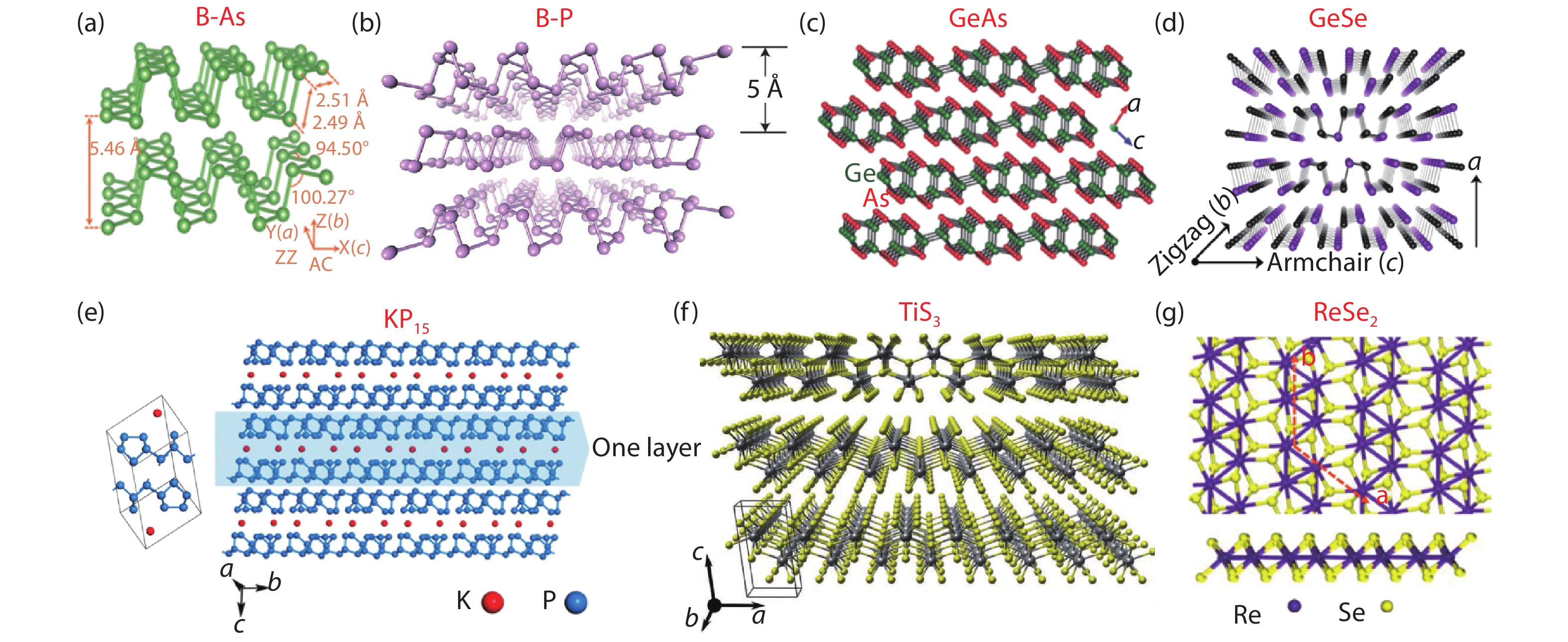
    Orthorhombic Black-Arsenic (B-As) (Fig. 1(a))[35] and Black-Phosphorus (B-P) (Fig. 1(b))[46] are the representative anisotropic materials belonging to the space group Bmab and Pcmn respectively. The bulk materials are the minerals in black color, so named for black-As and black-P[36]. In the single layer, each As or P atom are covalently bonded with three adjacent atoms. GeAs (Fig. 1(c)), similar to GaTe structure with the space group of C2/m, is the new 2D intralayer anisotropic material[47]. In the structure of GeAs, each Ge atoms are coordinated by one Ge atom and three As atoms, and each As atoms are coordinated by three Ge atoms. Therefore, there are two kinds of Ge–Ge bonds parallel and perpendicular to b-axis[40,47,50]. GeSe is the derivative of B-As and B-P and belongs to Pcmn- space group as shown in Fig. 1(d)[41]. KP15 is another kind of layered material with fiber-like structure. The left of Fig. 1(e) is the unit cell of KP15, and the right is the triclinic KP15 structure with the space group . As shown in the structure, one layer consists of two antiparallel P tubes, and four P tubes are coordinated by K atoms. Each K atom is coordinated with one [P15] cell. The inside of [P15] cell exhibits pentagonal P atoms arrangement which causes the highly anisotropic property[45]. Quasi-1D titanium trisulfide (TiS3) is shown in Fig. 1(f)[51]. There are two kinds of Ti-S bonds lengths in the structure, one is 4.97 Å along a-axis and another is 3.43 Å along b-axis[52]. Contrary to above materials, ReS2[53], ReS2(1–x)Se2x[49], and ReSe2[44, 54] belong to distorted 1T structure. The crystal structure of ReSe2 is shown in Fig. 1(g), in which diamond-shaped Re4 clusters along zigzag due to the Peierls transition.

    (Color online) Crystal structures of two-dimensional anisotropic materials, including (a) orthorhombic black-arsenic. Reproduced with permission[35]. Copyright 2018, John Wiley and Sons. (b) Orthorhombic black-phosphorus. Reproduced with permission[46]. Copyright 2014, Springer Nature. (c) Monoclinic GeAs. Reproduced with permission[47]. Copyright 2018, John Wiley and Sons. (d) Orthorhombic GeSe. Reproduced with permission[41]. Copyright 2017, American Chemical Society. (e) Triclinic KP15. Reproduced with permission[45]. Copyright 2018, American Chemical Society. (f) Monoclinic TiS3. Reproduced with permission[48]. Copyright 2018, Wiley-VCH. (g) Triclinic ReSe2. Reproduced with permission[49]. Copyright 2016, American Chemical Society.

    Figure 1.(Color online) Crystal structures of two-dimensional anisotropic materials, including (a) orthorhombic black-arsenic. Reproduced with permission[35]. Copyright 2018, John Wiley and Sons. (b) Orthorhombic black-phosphorus. Reproduced with permission[46]. Copyright 2014, Springer Nature. (c) Monoclinic GeAs. Reproduced with permission[47]. Copyright 2018, John Wiley and Sons. (d) Orthorhombic GeSe. Reproduced with permission[41]. Copyright 2017, American Chemical Society. (e) Triclinic KP15. Reproduced with permission[45]. Copyright 2018, American Chemical Society. (f) Monoclinic TiS3. Reproduced with permission[48]. Copyright 2018, Wiley-VCH. (g) Triclinic ReSe2. Reproduced with permission[49]. Copyright 2016, American Chemical Society.

    3. Anisotropy in Raman spectroscopy

    Raman spectroscopy is a fast, nondestructive and high sensitivity tool for the characterization of the lattice structure as well as the electronic, optical and phonon properties of 2D materials[5559]. Among them, the angle-resolved polarized Raman spectroscopy is necessary to be utilized to research crystal orientation and phonon anisotropy[60,61]. For angle-resolved polarized Raman spectroscopy, there are three typical configurations as shown in the Figs. 2(a)2(c). Fig. 2(a) is a schematic diagram of the most basic configurations for angle-resolved polarized Raman measurements. The polarization of incident laser is rotated with α degree by rotating the half-wave plate with α/2 degree respecting to the fast-axis direction. This configuration is widely used for its time-saving and easy-to-handle advantages. In Fig. 2(b), the laser polarization is fixed along y axis by a polarizer, and the analyzer direction is set to x axis or y axis, which corresponds to generally-used cross- or parallel-polarization configuration, respectively. In the process of measurement, the sample is clockwise rotated around z axis with β angle. The configuration of Fig. 2(c) is equivalent in function to that in Fig. 2(b) but different in geometry, where a half-wave plate is inserted between the edge filter and the objective while the sample is fixed[62]. This configuration can be a substitution of the former one since it can technically avoid sample moving and be more time-consuming.

    (Color online) Raman spectroscopy. (a)–(c) the schematic diagram of three typical polarized-Raman configurations. Reproduced with permission[62]. Copyright 2017, CPB. (d) The left is the Raman spectra of ReSe2 grown on hBN and SiO2 respectively. The right is the angular-dependent Raman intensity of 238 cm–1 shown in polar plot under different polarized-Raman configurations. Reproduced with permission[44]. Copyright 2018, American Chemical Society. (e) the angular-dependent Raman intensity of 212 and 406 cm–1 in ReS2(1–x)Se2x. Reproduced with permission[49]. Copyright 2016, American Chemical Society. (f) Angle-resolved polarized Raman spectra of KP15. The right picture is the intensity of peak 9. (g) Polarization-resolved PL intensity of KP15. The polar plots show the PL intensity of KP15 as the function of the detection angle and excitation angle respectively. Reproduced with permission[45]. Copyright 2018, American Chemical Society.

    Figure 2.(Color online) Raman spectroscopy. (a)–(c) the schematic diagram of three typical polarized-Raman configurations. Reproduced with permission[62]. Copyright 2017, CPB. (d) The left is the Raman spectra of ReSe2 grown on hBN and SiO2 respectively. The right is the angular-dependent Raman intensity of 238 cm–1 shown in polar plot under different polarized-Raman configurations. Reproduced with permission[44]. Copyright 2018, American Chemical Society. (e) the angular-dependent Raman intensity of 212 and 406 cm–1 in ReS2(1–x)Se2x. Reproduced with permission[49]. Copyright 2016, American Chemical Society. (f) Angle-resolved polarized Raman spectra of KP15. The right picture is the intensity of peak 9. (g) Polarization-resolved PL intensity of KP15. The polar plots show the PL intensity of KP15 as the function of the detection angle and excitation angle respectively. Reproduced with permission[45]. Copyright 2018, American Chemical Society.

    ReS2, ReSe2 and their alloy ReS2(1–x)Se2x are the emerging materials which exhibits a stable distorted 1T phase and strong in-plane anisotropy due to its reduced crystal symmetry. It is essential to research their angular-dependent anisotropy behaviors. The Raman spectra of ReSe2 with different thicknesses grown on SiO2 and hBN substrate are shown in the left of Fig. 2(d)[44]. With the thickness increasing, the peak positions are blue shift (2 cm–1) due to the decoupled lattice vibrations, which is similar to ReS2(1–x)Se2x. The angle-resolved polarized Raman intensity of ReSe2 at 238 cm–1 peak has displayed in the right of Fig. 2(d) under the configuration in Fig. 2(b). The periodic changes in intensity give direct illustration of its strong anisotropy. Fig. 2(e) shows the angle-resolved polarized Raman intensity of ReS2(1–x)Se2x at 212 cm–1 (red points) and 406 cm-1 (blue points) as the composition changes[49]. For the peak of 212 cm–1 in ReS2(1–x)Se2x, the direction with maximum intensity gradually deviates from b-axis direction (along Re chains) with x increasing. For the ReS2(1–x)Se2x crystals, the Raman tensor R of all Raman active modes have the form of . The intensity of Raman mode can be expressed by the function of , where and is the unit polarization vector for scattered light and excitation laser, respectively. Therefore, the intensity of polarized Raman can be written as . All experimental data can thus be well fitted[55].

    As for another layered material KP15 with distinctive shape, its Raman spectra (Fig. 2(f)) include 14 Raman peaks locating at 466.6, 449.0, 408.8, 376.3, 368.4, 351.1, 303.7, 288.5, 124.1, 114.1, 106.8, 90.7, 74.6 and 66.4 cm-1. The thickness of the measured sample is 373.9 nm. As the most anisotropic one, the angle-dependent Raman intensity of peak 9 is individually extracted and shown in the right of Fig. 2(f). All Raman peaks in Fig. 2(f) follow the function of cos6θ. In addition, the crystal of KP15, similar to phosphorene (P), also has anisotropic photoluminescence (PL) properties. In the measurement of polarization-resolved PL spectra, the KP15 samples of 373.9 nm and 2.3 μm are chosen and the results are shown in Fig. 2(g). Four kinds of excitation-detection combinations are taken in the polarization-resolved PL measurements. When the laser polarization is remained constant, the intensity ratio (y-axis/x-axis) is 5.8, which indicates the anisotropic emission property caused by its high anisotropic structure. From the polar plot in Fig. 2(g), it can be observed that the anisotropy of samples with different thickness is diverse from each other, which indicates that the anisotropy of PL spectra also relates to the thickness of the KP15[45].

    GeSe is a typically stable and anisotropic IV−VI chalcogenide. The angle-dependent Raman spectrum of GeSe is shown in the Fig. 3(a) with the corresponding contour color map under the parallel and cross polarization configurations. The contour map visually shows the anisotropy of each peak. The parallel-polarization configuration and cross-polarization configuration correspond to the polarization analyzer before the spectrometer parallel and perpendicular to the laser polarization, as mentioned before. The sample is rotated with a step of ten degrees. There are two Raman peaks around 150 and 188 cm–1 coming from B3g mode and Ag mode respectively. Similar to materials with anisotropic absorption such as B-P, one needs to consider the impact of light absorption in the form of the Raman tensor. Additional phase index should be introduced to fit the experimental results. In parallel-polarization configuration, the fitting function of Ag mode is , and that of B3g mode is . While under the cross-polarization configuration, the fitting function of Ag mode is f2sin22θ, and that of B3g is f2cos22θ[41].

    (Color online) (a) The angle-dependent Raman spectrum of GeSe and the corresponding contour color map in the parallel-polarization configuration (left) and cross-polarization configuration (right). Reproduced with permission[41]. Copyright 2017, American Chemical Society. (b) The Raman spectrum of B-As with laser polarized along different directions (up). The angle-resolved intensity of Ag1 and B2g-mode are extracted and shown in polar plot (down). Reproduced with permission[35]. Copyright 2018, John Wiley and Sons. (c) The Raman spectrum of GeAs in the non-polarized, parallel-polarized and cross-polarized configuration (left). The angle-dependent Raman spectrum of GeAs under traditional configuration (right). (d) The intensities of angle-dependent Raman peak are extracted and shown in the polar plot. Reproduced with permission[40]. Copyright 2018, American Chemical Society.

    Figure 3.(Color online) (a) The angle-dependent Raman spectrum of GeSe and the corresponding contour color map in the parallel-polarization configuration (left) and cross-polarization configuration (right). Reproduced with permission[41]. Copyright 2017, American Chemical Society. (b) The Raman spectrum of B-As with laser polarized along different directions (up). The angle-resolved intensity of Ag1 and B2g-mode are extracted and shown in polar plot (down). Reproduced with permission[35]. Copyright 2018, John Wiley and Sons. (c) The Raman spectrum of GeAs in the non-polarized, parallel-polarized and cross-polarized configuration (left). The angle-dependent Raman spectrum of GeAs under traditional configuration (right). (d) The intensities of angle-dependent Raman peak are extracted and shown in the polar plot. Reproduced with permission[40]. Copyright 2018, American Chemical Society.

    The anisotropic characteristics of angular-dependent and excitation-dependent Raman spectra of B-P has been thoroughly reviewed in previous work[61]. Similarly, B-As, a rare chemical form of arsenic, is also reported with extremely anisotropy. The angle-dependent Raman spectrum (Fig. 3(b)) can be used to investigate the anisotropic vibrational properties. The strong Raman peaks are located at 223.6, 230.2 and 257.9 cm–1, corresponding with out-of-plane Ag1, in-plane B2g and in-plane Ag2 modes. Among them, the intensity of Ag1 mode is fitted by the function of (1 + bsin2θ)2, where b is a matrix element in the Raman tensor of Ag1 mode. The intensity of B2g mode varies as e2sin2(2θ), where e is the Eiler’s number and θ is the angle between the laser polarization and AC direction of crystal. From the polar plot in Fig. 3(b), the Ag1 peak behave strongest in intensity and B2g weakest along the direction of armchair, which is consistent with the its electrical behaviors as discussed below.

    GeAs is a newly introduced 2D material with high anisotropy. From the Raman spectra taken under three configurations (Fig. 3(c)-left), it can be observed that the non-polarized Raman spectra includes 7 peaks (locating at 147, 174, 242, 256, 274, 283, 307 cm–1), and the parallel/cross configuration include 6 peaks/2 peaks, which confirms the intrinsic anisotropy of GeAs crystal. Furthermore, the angle-dependent Raman spectra is measured by rotating the sample under non-polarized configuration and shown in the Fig. 3(c)-right. The intensities of angle-dependent of Raman is extracted and shown in polar plot (Fig. 3(d)). In the polar plot, the data can be fitted by the function of , where θ represents the polarized angle and all of , and are fitting parameters[40, 63, 64].

    In addition, Prof. Dai and co-workers have researches the anisotropic Raman response of SnSe, MoTe2 and WTe2[6567].

    4. Electrical anisotropy and polarization-sensitive photodetectors

    The anisotropy along armchair (AC) and zigzag (ZZ) directions also manifest on their photoelectrical properties. For convenience of comparison, the details of a series 2D anisotropic materials are summarized and provided in Table 1. Conduction ratio is defined by dividing the maximum conduction value by the minimum conduction value showing along different orientation. Responsivity is the ratio of photocurrent generated by photoconductive mode to excitation light. Dichroic ratio represents the degree of the discrepancy in response to different polarized light by dividing the maximum photocurrent value by the minimum photocurrent value.

    Table Infomation Is Not Enable

    The anisotropic optical properties of B-P crystal have been researched detailly. The anisotropic optical absorptions of visible light and infrared light are measured under the configuration shown in the schematic diagram in Fig. 4(a). The optical absorptions (Fig. 4(b)) shows that more visible photons are absorbed with light polarized along x-axis (0°) than that along y-axis (90°). B-P photodetector with a ring-shaped photocurrent collector is fabricated (Fig. 4(c)-(1)) and its polarization-dependent photoresponsivity is shown in Fig. 4(c)-(2), with illumination from 400 mn to 1700 nm under the polarization along x crystal axis (0°) and y crystal axis (90°) respectively. The photoresponsivity contrast ratio between the two perpendicular directions is as large as 3.5. To clearly observe the anisotropic photoresponse, spatial mapping of photocurrent is obtained (Fig. 4(c)-(3)). It visually demonstrates the difference in intensity of photocurrent along the x-axis and y-axis[38].

    (Color online) (a) Schematic of the optical measurement under visible light (left-picture) and infrared light (right-picture). (b) Light absorption of B-P flake with different polarized light. (c) B-P photodetector with broadband response and polarization sensitivity. (1) The optical image of B-P photodetector with ring-electrode. (2) Polarization dependence of photoresponsivity from 400 to 1700 nm with polarization along x crystal axis (0°) and y crystal axis (90°). (3) The spatial mapping of photocurrent under polarization angle of 0 and 90 degree. Reproduced with permission[38]. Copyright 2015, Springer Nature. (d) The angle-dependent electrical conductance of B-As. The optical image of device for the anisotropic electrical measurements is inserted in it. (e) Temperature dependent resistance based on B-As Hall device shown in the inset(left). The magnetic field -dependent conductively and , corresponding with the direction of armchair and zigzag (right). Reproduced with permission[35]. Copyright 2018, John Wiley and Sons. (f) The Ids–Vds curves of As0.83P0.17 with illumination and dark environment along x axis and y axis. (g) The laser polarization-sensitive photocurrents of As0.83P0.17 in polar plot at Vds = 0 V (left). Photocurrent mapping of As0.83P0.17 at Vds = 0 V (right) when polarization direction parallels (0°) and perpendicular (90°) to the contact edge of the metal. Reproduced with permission[39]. Copyright 2017, American Association for the Advancement of Science.

    Figure 4.(Color online) (a) Schematic of the optical measurement under visible light (left-picture) and infrared light (right-picture). (b) Light absorption of B-P flake with different polarized light. (c) B-P photodetector with broadband response and polarization sensitivity. (1) The optical image of B-P photodetector with ring-electrode. (2) Polarization dependence of photoresponsivity from 400 to 1700 nm with polarization along x crystal axis (0°) and y crystal axis (90°). (3) The spatial mapping of photocurrent under polarization angle of 0 and 90 degree. Reproduced with permission[38]. Copyright 2015, Springer Nature. (d) The angle-dependent electrical conductance of B-As. The optical image of device for the anisotropic electrical measurements is inserted in it. (e) Temperature dependent resistance based on B-As Hall device shown in the inset(left). The magnetic field -dependent conductively and , corresponding with the direction of armchair and zigzag (right). Reproduced with permission[35]. Copyright 2018, John Wiley and Sons. (f) The IdsVds curves of As0.83P0.17 with illumination and dark environment along x axis and y axis. (g) The laser polarization-sensitive photocurrents of As0.83P0.17 in polar plot at Vds = 0 V (left). Photocurrent mapping of As0.83P0.17 at Vds = 0 V (right) when polarization direction parallels (0°) and perpendicular (90°) to the contact edge of the metal. Reproduced with permission[39]. Copyright 2017, American Association for the Advancement of Science.

    B-As, as a “cousin” of B-P, is reported as high mobilities and anisotropic behaviors. The anisotropic research is mainly focused on the direction of armchair and zigzag. For an anisotropic semiconductor with twofold symmetry in the polar plot, the conductance (S) varies with the θ changing as Sθ = Smaxcos2θ + Sminsin2θ[35]. From fitting the angle-dependent electrical conductance in Fig. 4(d), the highest conduction is Smax = 24.3 μS along armchair direction, and the weakest is Smax = 3.8 μS along zigzag direction. The anisotropic conduction ratio is as high as 6.4. To further analysis its anisotropic electric properties, the hall device is fabricated to measure the temperature dependent resistance (R) and magnetic dependent conductively (σ) along armchair and zigzag directions. The resistance is sensitive to temperature along zigzag while inert along armchair, with a much higher value along zigzag compared to armchair, as shown in Fig. 4(e)-left. As the same time, the magnetic dependent conductively shows opposite signs along armchair and zigzag. Herein, the longitudinal conductivities can be described as , and the transverse conductivities as . In the Fig. 4(e)-right, the results of magnetic field dependent conductively can be fitted as the function of and . And then, the concentration (n) and mobility (μ) of holes (h) and electrons (e) can be extracted from above equations. The obtained concentration are ne = 2.0 × 1016 cm–3 and nh = 5.3 × 1015 cm–3 while mobility are as high as μhZZ = 60.7 cm2V–1s–1 and μeZZ = 376.7 cm2V–1s–1 along zigzag direction, μhAC = 10 606 cm2V–1s–1 and μeAC = 1.5 cm2V–1s–1 along armchair direction[35].

    Orthorhombic black-AsP, which is the alloy of B-As and B-P, is fabricated by the Prof. Hu and co-workers[39]. For the polarization-dependent photocurrent and the polarization-sensitive photocurrent mapping (Fig. 4(g)), researchers focused on the properties along x-axis (armchair direction) and y-axis (zigzag direction). The polarization-dependent photocurrent was measured under the illumination of linear-polarized light. The laser was set to pass a linear polarizer to obtain the linear-polarized light, and the half-wave plate to adjust the polarization direction, then the 20× or 100× microscopy objective to focus. The polarization-sensitive photocurrent mapping is measured by scanning the linear-polarized light over the device. At the dark environment, the conductivity along x-axis is nearly 1.73 times than that along y-axis at Vg= 0 V, which is consistent with previously reported results[74]. Under the illumination of mid-infrared laser (4.034 μm), the anisotropic photocurrent ratio IPx/IPy at Vds= 1 V is nearly 3.51. The photocurrent was observed to be maximum when the light polarization was along the x-direction and minimum when the light was along the y-direction, similar to the observation in black phosphorus[39]. The photocurrent anisotropy ratio is as high as γ= (IpmaxIpmin)/(Ipmax + Ipmin) ≈ 0.59, which is larger than the ratio of B-P (~0.3)[17].

    GeAs crystal, as a new 2D materials, is reported by its highly anisotropic electricity and photoelectricity properties. The field-effect mobility (Fig. 5(b)) of GeAs transistors are measured with a resolution of 15° under vacuum of 10–5 Torr. The mobility is calculated by the equation of , where Cox= 11.6 Nf/cm2 corresponds with 300 nm SiO2 dielectric capacitance, L and W is the channel length and width, G represents the channel conductance, and VG is the voltage of gate. The anisotropic mobility ratio is as high as 4.8[47]. From the polarization-resolved absorption spectra (Fig. 5(c)), it can be observed that a linear dichroism photodetection behavior and the dichroic ratio is 1.14/1.42 at 520 nm/830 nm respectively. The direction of the strongest absorption is dominating along b-axis between 400 to 500 nm wavelength while reverses to a-axis after 630 nm wavelength. Comparing the absorption of visible light with near-infrared light, the angle of strongest absorption direction is around 80 degrees. This phenomenon is defined as perpendicular optical reversal phenomenon.

    (Color online) The properties of electricity and photoelectricity. (a) The optical image of GeAs for angle-dependent transporting measurement. (b) The anisotropic field-effect mobility in polar plot. Reproduced with permission[47]. Copyright 2018, John Wiley and Sons. (c) Angle-resolved absorption spectra of GeAs from 400 to 2000 nm. (d) The schematic diagram of polarized photodetection devices. (e) The polarization-sensitive photocurrents in polar plot under 520 and 830 nm laser. (f) The mapping of polarization-dependent photocurrent under 520 and 830 nm laser. Reproduced with permission[40]. Copyright 2018, American Chemical Society. (g) Polarization-resolved experimental absorption spectra of GeSe from 400 to 950 nm. (h) The colormap of anisotropic photo response under the 808 nm laser. x-axis represents the voltage of source and drain, y-axis represents the polarized angle, and Iph is denoted by the color bar. (i) The data of polarized Iph are extracted and shown in polar plot. Reproduced with permission[41]. Copyright 2017, American Chemical Society.

    Figure 5.(Color online) The properties of electricity and photoelectricity. (a) The optical image of GeAs for angle-dependent transporting measurement. (b) The anisotropic field-effect mobility in polar plot. Reproduced with permission[47]. Copyright 2018, John Wiley and Sons. (c) Angle-resolved absorption spectra of GeAs from 400 to 2000 nm. (d) The schematic diagram of polarized photodetection devices. (e) The polarization-sensitive photocurrents in polar plot under 520 and 830 nm laser. (f) The mapping of polarization-dependent photocurrent under 520 and 830 nm laser. Reproduced with permission[40]. Copyright 2018, American Chemical Society. (g) Polarization-resolved experimental absorption spectra of GeSe from 400 to 950 nm. (h) The colormap of anisotropic photo response under the 808 nm laser. x-axis represents the voltage of source and drain, y-axis represents the polarized angle, and Iph is denoted by the color bar. (i) The data of polarized Iph are extracted and shown in polar plot. Reproduced with permission[41]. Copyright 2017, American Chemical Society.

    Further, the polarization-resolved photocurrents of GeAs is measured under the schematic configuration in Fig. 5(d), where linear-polarized laser is obtained with the polarizer and its polarization is changed by half-wave plate. By rotating the half-wave plate with α/2 steps, the angle-resolved photocurrents are measured and shown in polar plot with α steps (Fig. 5(e)). The dichroic ratio ( ) is as high as 1.49 at 520 nm laser illumination and 4.4 at 830 nm laser illumination. The fitting curves of polarization-resolved photocurrents follow the function of Iph(θ) = Ipmaxcos2(θ + φ) + Ipminsin2(θ + φ), where only φ is the adjustable fitting parameter. The perpendicular optical reversal phenomenon is also observed in the photoelectric measurement with the reversal angle is 70°, corresponding with the anisotropic absorption spectra.

    To research the source of photocurrent, the spatial mapping of photocurrents is measured with different polarization directions (Fig. 5(f)). Once again, distinct angle difference for linear-polarization mapping was observed around 80° between 520 and 830 nm lasers, corresponding with the reverse angle observed in anisotropic absorption spectra and polarization-resolved photocurrents. Besides, it is can be observed that the photocurrent signals occur in the interface between GeAs nanoflake and electrode, and two contacts have opposite polarity. That is due to the Schottky junction, formed between semiconductor materials and metal electrode, causing the photovoltaic and photothermoelectric effect. It is similar to the Schottky diode[40].

    The distinct anisotropic features of GeSe is manifested in linear-polarization-sensitive photodetectors. The polarization-resolved absorption spectra of GeSe with 49.6 nm thicknesses is probed (Fig. 5(g)). The results show that the absorption ratio , 1.26 and 3.02 at the wavelength of 532, 638 and 808 nm, respectively. There is a polarization peak around the wavelength of 808 nm which corresponds with the electric band structure of GeSe crystal. Further, by measuring the layer-dependent photo response, it is found that the photo response of the 8–16 nm GeSe have the best results. So, the 8.63 nm GeSe is chosen to measure the properties of polarization photodetectors. The colormap (Fig. 5(h)) directly exhibits the relationship between the photo response and the angle of polarized laser under the illumination of 808 nm laser. The polarization photocurrents under 95 mW/cm2 illumination and voltage of source–drain of 2 V are measured and shown in polar plot (Fig. 5(i)). The data of polarization photocurrents can be fitted by the function . The dichroic ratio of photo response is at 808 nm laser. The dichroic ratio of absorption and photo response is different, which is possibly due to defect states introduced by the processing fabrication, measuring apparatus error or different thickness samples and so on[41].

    ReSe2 crystal is different from other hexagonal TMDs, and its anisotropy is introduced by the 1T phase of 1D arrangement of Re chains. From the polarization sensitive transmission spectra in Fig. 6(a), it can be observed that the infrared transmission spectrum with γ = 0° is more dipping than that with γ = 90° at the energy between 1.32 and 1.85 eV. The γ = 0° is defined as the direction of polarization light parallel to the b-axis, and the γ = 90° is defined as the direction of polarization light perpendicular to the b-axis. Besides, the anisotropic transmission ratio at 1.86 eV is 0.66 and 0.98 with γ = 0° and 90°, which demonstrating b-axis absorb more photons. Further, polarization-dependent photocurrent mappings are measured in order to find the source of the photocurrent. It can be seen that photocurrent signals come from the ReSe2 channel rather than the metal electrodes, which confirms that the influence of Schottky barriers are eliminated[44]. Next, a series of optical anisotropies of ReS2(1–x)Se2x were researched (Fig. 6 (c))[49]. It can be seen that the mobility of ReSe2, ReS0.38Se1.62, and ReS1.02Se0.98 is in the range of 2.12 to 6.16, 1.44 to 5.53, and 1.26 to 8.45 cm2 V−1 s−1, respectively[75]. The maximum mobility of ReS2(1–x)Se2x are along b-axis. At the same time, the anisotropic mobility ratios of ReSe2, ReS0.38Se1.62, and ReS1.02Se0.98 few-layers are calculated to be 2.9, 3.8 and 5.6, respectively[76].

    (Color online) (a) The polarization sensitive transmission spectra of ReSe2 nanoflake. (b) Polarization dependent photocurrent mapping based on ReSe2 FET. The thickness of the ReSe2 channel is 12 nm. Reproduced with permission[44]. Copyright 2016, American Chemical Society. (c) Angle-dependent mobility of ReSe2, ReS0.38Se1.62 and ReS1.02Se0.98 alloys. Reproduced with permission[48]. Copyright 2017, John Wiley and Sons. (d) The polarization-sensitive transmittance spectra of a TiS3 crystal from 400 to 1000 nm (up-picture). Polar plot of the transmittance at 500, 600, 700, 800 nm wavelengths (down-picture). (e) I–V curves of the TiS3/Si-based device under the illumination of linearly polarized laser (660 nm). (f) Two polar plots of polarization-sensitive light currents under the bias voltage of –2 V (left-picture) and 0 V (right-picture). Reproduced with permission[48]. Copyright 2018, Wiley-VCH.

    Figure 6.(Color online) (a) The polarization sensitive transmission spectra of ReSe2 nanoflake. (b) Polarization dependent photocurrent mapping based on ReSe2 FET. The thickness of the ReSe2 channel is 12 nm. Reproduced with permission[44]. Copyright 2016, American Chemical Society. (c) Angle-dependent mobility of ReSe2, ReS0.38Se1.62 and ReS1.02Se0.98 alloys. Reproduced with permission[48]. Copyright 2017, John Wiley and Sons. (d) The polarization-sensitive transmittance spectra of a TiS3 crystal from 400 to 1000 nm (up-picture). Polar plot of the transmittance at 500, 600, 700, 800 nm wavelengths (down-picture). (e) IV curves of the TiS3/Si-based device under the illumination of linearly polarized laser (660 nm). (f) Two polar plots of polarization-sensitive light currents under the bias voltage of –2 V (left-picture) and 0 V (right-picture). Reproduced with permission[48]. Copyright 2018, Wiley-VCH.

    In 2017, Prof. Wei and co-workers successfully synthesized the TiS3 crystal and researched its anisotropic optical properties. The crystal TiS3 is formed by interacting quasi-1D chains and the weakly coupled Ti–S bond. The Ti–S bond of TiS3 is nearly 80% less than that of TiS6 polyhedrons within the chain. This leads to the strong anisotropy in TiS3. Further, the anisotropic photocurrents are measured with different wavelengths of laser illumination and shown marked linear dichroism. The extinction ratios based on TiS3 photodetector are calculated to be 2.8, 4.6 and 4.0 under the illumination of 532, 638 and 830 polarized light[52,77]. In 2018, Andres Castellanos-Gomez and co-works researched the polarization optical properties of TiS3/Si p–n junction[48]. In their work, the TiS3 nanowire is deposited onto PDMS to measure its polarization-sensitive transmittance spectra, as shown in Fig. 6(d). In the transmittance spectra, the 0 degree corresponds to a-axis, and 90 degrees corresponds to b-axis. At 2.32 eV, the transmittance along the a-axis reaches 71%, as the same time, the transmittance along the b-axis is as low as 52%. The polarization-sensitive transmittance of typical wavelengths (500, 600, 700 and 800 nm) are extracted and shown in the polar plot (the inset of Fig. 6(d)), which indicates the in-plane optical properties of TiS3 crystal. Then, the photocurrents of TiS3/Si-based device are measured with the 660 nm polarizer laser (Fig. 6(e)). The polarizer photocurrents under –2 and 0 V bias voltage are extracted and shown in the Fig. 6(f).

    Furthermore, the anisotropies of electrical in SnSe and Ta2NiS5 have been investigated. The condition radio of SnSe can be as high as 3.9[67]. And the condition radio of Ta2NiS5 is 1.78 at 80 K and 1.41 at 293 K[78].

    5. Conclusion

    In this review, we have reviewed several two-dimensional anisotropic materials and related field effect transistors and photodetectors based on recent advances. This review pays special attention and make comparison of the anisotropy in their optical and electrical properties. More anisotropic materials are gradually revealed and can be broadly applicable to various platforms and devices. Polarization-sensitive photodetectors based on such anisotropic crystals have fast, high sensitivity, broad spectrum, high anisotropy ratio and greatly repeated anisotropic properties. We hope this review could guide interested readers to properly utilize their anisotropic behaviors for material synthesis and specific applications.

    Acknowledgment

    This work was financially supported by the National Natural Science Foundation of China (Grant Nos. 61622406, 61571415, 11874350, 11434010), and the Strategic Priority Research Program of Chinese Academy of Sciences (Grant No. XDB30000000).

    References

    [1] J Shang, L Huang, Z Wei. Effects of vertical electric field and compressive strain on electronic properties of bilayer ZrS2. J Semicond, 38, 033001(2017).

    [2] C Fan, Y Li, F Lu et al. Wavelength dependent UV–vis photodetectors from SnS2 flakes. RSC Adv, 6, 422(2016).

    [3] Z Wei, B Li, C Xia et al. Various structures of 2D transition-metal dichalcogenides and their applications. Small Methods, 2, 1800094(2018).

    [4] X Wang, Y Cui, T Li et al. Recent advances in the functional 2D photonic and optoelectronic devices. Adv Opt Mater, 1801274(2018).

    [5] Y Wang, L H Huang, B Li et al. Composition-tunable 2D SnSe2(1−x)S2x alloys towards efficient bandgap engineering and high performance (opto)electronics. J Mater Chem C, 5, 84(2017).

    [6] T Mueller, F Xia, P Avouris. Graphene photodetectors for high-speed optical communications. Nat Photon, 4, 297(2010).

    [7] K S Novoselov, A K Geim, S V Morozov et al. Two-dimensional gas of massless Dirac fermions in graphene. Nature, 438, 197(2005).

    [8] L Huang, L Tao, K Gong et al. Role of defects in enhanced Fermi level pinning at interfaces between metals and transition metal dichalcogenides. Phys Rev B, 96, 205303(2017).

    [9] V Podzorov, M Gershenson, C Zeis et al. High-mobility field-effect transistors based on transition metal dichalcogenides. Appl Phys Lett, 84, 3301-3303(2004).

    [10] C Xia, J Li. Recent advances in optoelectronic properties and applications of two-dimensional metal chalcogenides. J Semicond, 37, 051001(2016).

    [11] N Huo, Y Yang, J Li. Optoelectronics based on 2D TMDs and heterostructures. J Semicond, 38, 031002(2017).

    [12] Q H Tan, X Zhang, X D Luo et al. Layer-number dependent high-frequency vibration modes in few-layer transition metal dichalcogenides induced by interlayer couplings. J Semicond, 38, 031006(2017).

    [13] Z Lou, Z Liang, G Shen. Photodetectors based on two dimensional materials. J Semicond, 37, 091001(2016).

    [14] M Amani, E Regan, J Bullock et al. Mid-wave infrared photoconductors based on black phosphorus-arsenic alloys. ACS Nano, 11, 11724(2017).

    [15] M Amani, C Tan, G Zhang et al. Solution-synthesized high-mobility tellurium nanoflakes for short-wave infrared photodetectors. ACS Nano, 12, 7253(2018).

    [16] F Chu, M Chen, Y Wang et al. A highly polarization sensitive antimonene photodetector with a broadband photoresponse and strong anisotropy. J Mater Chem C, 6, 2509(2018).

    [17] T Hong, B Chamlagain, W Lin et al. Polarized photocurrent response in black phosphorus field-effect transistors. Nanoscale, 6, 8978(2014).

    [18] N Huo, S Yang, Z Wei et al. Photoresponsive and gas sensing field-effect transistors based on multilayer WS(2) nanoflakes. Sci Rep, 4, 5209(2014).

    [19] J Lai, X Liu, J Ma et al. Anisotropic broadband photoresponse of layered type-II Weyl semimetal MoTe2. Adv Mater, 30, e1707152(2018).

    [20] Y Li, Y Wang, L Huang et al. Anti-ambipolar field-effect transistors based on few-layer 2D transition metal dichalcogenides. ACS Appl Mater Interfaces, 8, 15574(2016).

    [21] Y Wang, L Huang, Z Wei. Photoresponsive field-effect transistors based on multilayer SnS2 nanosheets. J Semicond, 38, 034001(2017).

    [22] T Cao, Z Li, D Y Qiu et al. Gate switchable transport and optical anisotropy in 90 degrees twisted bilayer black phosphorus. Nano Lett, 16, 5542(2016).

    [23] B Liu, M Kopf, A N Abbas et al. Black arsenic-phosphorus: layered anisotropic infrared semiconductors with highly tunable compositions and properties. Adv Mater, 27, 4423(2015).

    [24] M Zhong, X Wang, S Liu et al. High-performance photodetectors based on Sb2S3 nanowires: wavelength dependence and wide temperature range utilization. Nanoscale, 9, 12364(2017).

    [25] L Ye, P Wang, W Luo et al. Highly polarization sensitive infrared photodetector based on black phosphorus-on-WSe2 photogate vertical heterostructure. Nano Energy, 37, 53(2017).

    [26] M Zhong, K Zhou, Z Wei et al. Highly anisotropic solar-blind UV photodetector based on large-size two-dimensional α-MoO3 atomic crystals. 2D Mater, 5, 035033(2018).

    [27] J B Li, X R Wang. Preface to the special topic on 2D materials and devices. J Semicond, 38, 031001(2017).

    [28] Z Hu, Q Li, B Lei et al. Abnormal near-infrared absorption in 2D black phosphorus induced by Ag nanoclusters surface functionalization. Adv Mater, 1801931(2018).

    [29] T Lin, X Cong, M L Lin et al. The phonon confinement effect in two-dimensional nanocrystals of black phosphorus with anisotropic phonon dispersions. Nanoscale, 10, 8704(2018).

    [30] C Barreteau, B Michon, C Besnard et al. High-pressure melt growth and transport properties of SiP, SiAs, GeP, and GeAs 2D layered semiconductors. J Cryst Growth, 443, 75(2016).

    [31] L Li, W Wang, P Gong et al. 2D GeP: An unexploited low-symmetry semiconductor with strong In-plane anisotropy. Adv Mater, 30, e1706771(2018).

    [32] B Mortazavi, T Rabczuk. Anisotropic mechanical properties and strain tuneable band-gap in single-layer SiP, SiAs, GeP and GeAs. Physica E, 103, 273(2018).

    [33] C Li, S Wang, C Li et al. Highly sensitive detection of polarized light using a new group IV–V 2D orthorhombic SiP. J Mater Chem C, 6, 7219(2018).

    [34] X Wang, A Jones, K Seyler et al. Highly anisotropic and robust excitons in monolayer black phosphorus. Nat Nanotechnol, 10, 517(2015).

    [35] Y Chen, C Chen, R Kealhofer et al. Black arsenic: a layered semiconductor with extreme in-plane anisotropy. Adv Mater, 30, 1800754(2018).

    [36] M Zhong, Q Xia, L Pan et al. Thickness-dependent carrier transport characteristics of a new 2D elemental semiconductor: black arsenic. Adv Funct.Mater, 28, 1802581(2018).

    [37] J A Silva-Guillén, E Canadell, P Ordejón et al. Anisotropic features in the electronic structure of the two-dimensional transition metal trichalcogenide TiS3: electron doping and plasmons. 2D Mater, 4, 025085(2017).

    [38] H Yuan, X Liu, F Afshinmanesh et al. Polarization-sensitive broadband photodetector using a black phosphorus vertical p–n junction. Nat Nanotechnol, 10, 707(2015).

    [39] M Long, A Gao, P Wang et al. Room temperature high-detectivity mid-infrared photodetectors based on black arsenic phosphorus. Sci Adv, 3, e1700589(2017).

    [40] Z Zhou, M Long, L Pan et al. Perpendicular optical reversal of the linear dichroism and polarized photodetection in 2D GeAs. ACS Nano(2018).

    [41] X Wang, Y Li, L Huang et al. Short-wave near-infrared linear dichroism of two-dimensional germanium selenide. J Am Chem Soc, 139, 14976(2017).

    [42] Y C Lin, H P Komsa, C H Yeh et al. Single-layer ReS(2): two-dimensional semiconductor with tunable in-plane anisotropy. ACS Nano, 9, 11249(2015).

    [43] E Zhang, Y Jin, X Yuan et al. ReS2-based field-effect transistors and photodetectors. Adv Funt Mater, 25, 4076(2015).

    [44] E Zhang, P Wang, Z Li et al. Tunable ambipolar polarization-sensitive photodetectors based on high-anisotropy ReSe2 nanosheets. ACS Nano, 10, 8067(2016).

    [45] N Tian, Y Yang, D Liu et al. High anisotropy in tubular layered exfoliated KP15. ACS Nano, 12, 1712(2018).

    [46] L Li, Y Yu, GJ Ye et al. Black phosphorus field-effect transistors. Nat Nanotechnol, 9, 372(2014).

    [47] J Guo, Y Liu, Y Ma et al. Few-layer GeAs field-effect transistors and infrared photodetectors. Adv Mater, 30, 1705934(2018).

    [48] Y Niu, R Frisenda, E Flores et al. Polarization-sensitive and broadband photodetection based on a mixed-dimensionality TiS3/Si p–n junction. Adv Optical Mater, 6, 1800351(2018).

    [49] W Wen, Y Zhu, X Liu et al. Anisotropic spectroscopy and electrical properties of 2D ReS2(1–x)Se2x. alloys with distorted 1T structure. Small, 13, 1603788(2017).

    [50] J W Rau, C R Kannewurf. Optical absorption, reflectivity, and electrical conductivity in GeAs and GeAs2. Phys Rev B, 3, 2581(1971).

    [51] P Wang, S Liu, W Luo et al. Arrayed Van Der Waals broadband detectors for dual-band detection. Adv Mater, 29(2017).

    [52] S Liu, W Xiao, M Zhong et al. Highly polarization sensitive photodetectors based on quasi-1D titanium trisulfide (TiS3). Nanotechnology, 29, 184002(2018).

    [53] M Rahman, K Davey, S Z Qiao. Advent of 2D rhenium disulfide (ReS2): fundamentals to applications. Adv Funct Mater, 27, 1606129(2017).

    [54] B Kang, Y Kim, JH Cho et al. Ambipolar transport based on CVD-synthesized ReSe2. 2D Mater, 4, 025014(2017).

    [55] X Zhang, Q H Tan, J B Wu et al. Review on the Raman spectroscopy of different types of layered materials. Nanoscale, 8, 6435(2016).

    [56] G Yang, W Zhang. Renaissance of pyridine-oxazolines as chiral ligands for asymmetric catalysis. Chem Soc Rev, 47, 1783(2018).

    [57] J B Wu, H Zhao, Y Li et al. Monolayer molybdenum disulfide nanoribbons with high optical anisotropy. Adv Opt Mater, 4, 756(2016).

    [58] J B Wu, M L Lin, X Cong et al. Raman spectroscopy of graphene-based materials and its applications in related devices. Chem Soc Rev, 47, 1822(2018).

    [59] L Liang, J Zhang, B G Sumpter et al. Low-frequency shear and layer-breathing modes in Raman scattering of two-dimensional materials. ACS Nano, 11, 11777(2017).

    [60] H Zhao, J Wu, H Zhong et al. Interlayer interactions in anisotropic atomically thin rhenium diselenide. Nano Res, 8, 3651(2015).

    [61] H B Ribeiro, M A Pimenta, C J S de Matos. Raman spectroscopy in black phosphorus. J Raman Spectrosc, 49, 76(2018).

    [62] X L Liu, X Zhang, M L Lin et al. Different angle-resolved polarization configurations of Raman spectroscopy: A case on the basal and edge plane of two-dimensional materials. Chin Phys B, 26, 067802(2017).

    [63] K Lee, S Kamali, T Ericsson et al. GeAs: Highly anisotropic van der Waals thermoelectric material. Chem Mater, 28, 2776(2016).

    [64] L Zhou, Y Guo, J Zhao. GeAs and SiAs monolayers: novel 2D semiconductors with suitable band structures. Phys E, 95, 149(2018).

    [65] Q Song, H Wang, X Pan et al. Anomalous in-plane anisotropic Raman response of monoclinic semimetal 1 T -MoTe2. Sci Rep, 7, 1758(2017).

    [66] Q Song, H Wang, X Xu et al. The polarization-dependent anisotropic Raman response of few-layer and bulk WTe2 under different excitation wavelengths. RSC Adv, 6, 103830(2016).

    [67] X Xu, Q Song, H Wang et al. In-plane anisotropies of polarized raman response and electrical conductivity in layered tin selenide. ACS Appl Mater Interfaces, 9, 12601(2017).

    [68] X Liu, C R Ryder, S A Wells et al. Resolving the in-plane anisotropic properties of black phosphorus. Small Methods, 1, 1700143(2017).

    [69] P Venuthurumilli, P Ye, X Xu. Plasmonic resonance enhanced polarization-sensitive photodetection by black phosphorus in near infrared. ACS Nano, 12, 4861(2018).

    [70] C Niu, P M Buhl, G Bihlmayer et al. Two-dimensional topological crystalline insulator and topological phase transition in TlSe and TlS monolayers. Nano Lett, 15, 6071(2015).

    [71] J Lai, Y Liu, J Ma et al. Broadband anisotropic photoresponse of the "hydrogen atom" version type-II Weyl semimetal candidate TaIrTe4. ACS Nano, 12, 4055(2018).

    [72] J Jiang, Z K Liu, Y Sun et al. Signature of type-II Weyl semimetal phase in MoTe2. Nat Commun, 8, 13973(2017).

    [73] W Zhou, J Chen, H Gao et al. Anomalous and polarization-sensitive photoresponse of Td–WTe2 from visible to infrared light. Adv Mater, 31, e1804629(2019).

    [74] F Xia, H Wang, Y Jia. Rediscovering black phosphorus as an anisotropic layered material for optoelectronics and electronics. Nat Commun, 5, 4458(2014).

    [75] F Cui, Q Feng, J Hong et al. Synthesis of large-size 1T' ReS2xSe2(1–x) alloy monolayer with tunable bandgap and carrier type. Adv Mater, 29, 1705015(2017).

    [76] X Meng, Y Zhou, K Chen et al. Anisotropic saturable and excited-state absorption in bulk ReS2. Adv Opt Mater, 6, 1800137(2018).

    [77] H Zheng, M Zhu, J Zhang et al. A first-principles study on the magnetic properties of Sc, V, Cr and Mn-doped monolayer TiS3. RSC Adv, 6, 55194(2016).

    [78] L Li, P Gong, W Wang et al. Strong in-plane anisotropies of optical and electrical response in layered dimetal chalcogenide. ACS Nano, 11, 10264(2017).

    Ziqi Zhou, Yu Cui, Ping-Heng Tan, Xuelu Liu, Zhongming Wei. Optical and electrical properties of two-dimensional anisotropic materials[J]. Journal of Semiconductors, 2019, 40(6): 061001
    Download Citation