High-resolution multi-color printing relies upon pixelated optical nanostructures, which is crucial to promote color display by producing nonbleaching colors, yet requires simplicity in fabrication and dynamic switching. Antimony trisulfide (Sb2S3) is a newly rising chalcogenide material that possesses prompt and significant transition of its optical characteristics in the visible region between amorphous and crystalline phases, which holds the key to color-varying devices. Herein, we proposed a dynamically switchable color printing method using Sb2S3-based stepwise pixelated Fabry-Pérot (FP) cavities with various cavity lengths. The device was fabricated by employing a direct laser patterning that is a less time-consuming, more approachable, and low-cost technique. As switching the state of Sb2S3 between amorphous and crystalline, the multi-color of stepwise pixelated FP cavities can be actively changed. The color variation is due to the profound change in the refractive index of Sb2S3 over the visible spectrum during its phase transition. Moreover, we directly fabricated sub-50 nm nano-grating on ultrathin Sb2S3 laminate via microsphere 800-nm femtosecond laser irradiation in far field. The minimum feature size can be further decreased down to ~45 nm (λ/17) by varying the thickness of Sb2S3 film. Ultrafast switchable Sb2S3 photonic devices can take one step toward the next generation of inkless erasable papers or displays and enable information encryption, camouflaging surfaces, anticounterfeiting, etc. Importantly, our work explores the prospects of rapid and rewritable fabrication of periodic structures with nano-scale resolution and can serve as a guideline for further development of chalcogenide-based photonics components.
Introduction
A color filter (CF), either reflective or transmissive, is treated as a crucial part of smart windows, complementary metal oxide semiconductor (CMOS) images, nano-displays, and solar-cell applications1-3. Colorant pigments employed as the main technique to produce on-chip color filters4 are forbidden by the relatively low resolution, high process cost, and short color durability. Structural colors are exceptional substitutes for colorant pigments since a gamut of colors is produced in a broad range of materials by engineering nanostructure geometry. Advanced nanofabrication techniques can obtain well-defined pixelated nanostructures with controlled geometry, size, and arrangement. The color response of these nanostructures can be manipulated by engineering photonic resonance or optical interference effects5. Compared to traditional dyes and pigments, the structural colors have the advantages of higher pixel resolution6, lower cost, higher data density7, higher compactness, higher resistance to heat and chemicals, better color tunability8, and improved stability without color fading7-12. However, thus far, most of the efforts have been put into static color printing5. It is inevitable and important to launch a change toward dynamic color printing since it takes much richer information and enables more advanced functionality. There are a few strategies to produce dynamic color printing using photonics nanostructures based on tunable optical properties via electrowetting solvents13 and liquid crystals14; redox reaction in dielectric via individual particles15, electrochromic polymers16, metal hydrogenation17; and mechanical actuation via stretching18 or applied external magnetic fields19. While electrical techniques to vary colors are arguably the most feasible for color displays20, laser writing can induce faster transiting and be employed in cases in which electronic control is not possible.
Chalcogenide phase change materials (CPCMs), broadly employed in solid-state electronic storage and DVDs21, 22, have recently attracted much attention for the tunable photonics devices in the spectrum ranging from the visible to near-infrared23-25. Of specific interest is a subwavelength ultrathin laminate of optically lossy dielectric on a metal mirror whose colors are sensitive to the permittivity and thickness of these dielectric laminates alone26, 27. With sub-nanosecond structural state transitions inducing large variations in their permittivities, CPCMs offer prompt and stable color variations between amorphous and crystalline phases. Yet, most of the CPCMs possess tiny permittivity variation, accordingly, a narrow spectral shift of ~50 nm in the visible spectrum when transited between the structural phases28, 29. Antimony trisulfide (Sb2S3), typical alloys in the chalcogenide family, are suitable for visible photonics owing to its high index contrast of ~1, good stability under room temperature, wide bandgap, and far less loss compared to generally employed CPCMs in the visible30. Planar heterostructure designs integrating Sb2S3 with a metal reflector have been proposed for solar cell devices31. Very recently, it has been shown that the broad bandgap Sb2S3 is desirable for a planar color-changing film32. Although laser writing is effective in producing rewritable CPCM color microprints, rare work explores its capability of generating stepwise pixelated Fabry−Pérot (FP) cavity array, which can produce precisely tunable structural color pixel by pixel via the selective reflection of visible light.
Herein, we have experimentally realized a lithography-free dynamically switchable color reflector by incorporating Sb2S3 within an asymmetric stepwise pixelated FP cavity array. More explicitly, the femtosecond (fs) laser has been employed to fabricate the asymmetric FP cavity array consisting of the stepwise Sb2S3 film sandwiched by a 100 nm thick gold (Au) reflector and air. We have demonstrated that the height of the Sb2S3 film cavity can be engineered by modulating the power of fs laser irradiation. These pixelated FP cavities with various cavity height (namely the thickness of Sb2S3 film) can produce a robust, vivid color palette owing to the interaction of the light in the multilayered structure. The reflectance can be continuously tuned over the whole visible spectrum by engineering the thickness of the Sb2S3 layer within the cavity. The Sb2S3 is used as the active dielectric to dynamically modulate the reflected color by transiting the state of Sb2S3 with 800-nm wavelength and 150-fs duration laser pulses. We have then presented a Bing Dwen Dwen microprint based on the stepwise pixelated FP cavity array, where the high-resolution color of the image can be dynamically changed via the phase transition of Sb2S3. Although the Abbe diffraction limit for the lithography-free laser writing is ~1876 nm33, we have successfully patterned lines with a minimum feature size down to ~45 nm (λ/17) by using microsphere femtosecond laser irradiation in far field. Such a super-resolution laser writing scheme is based on the co-effect of microsphere focusing, top threshold effect, two-photons absorption, and high-repetition-rate fs laser-induced incubation effect. Moreover, our color reflector does not need any complex lithographic techniques during the fabrication, which significantly reduces the complexity and device cost. These color-varying devices based on the CPCM may pave the path toward the next generation of inkless erasable papers or displays and offer camouflaging surfaces, compact systems, and signaling to engineer the spectrum of visible light.
Materials and methods
Sample fabrication
We first clean a silicon (Si) wafer using acetone, isopropyl alcohol, and water in an ultrasonicator. We deposit a 100 nm-thick Au layer onto the Si (001) substrate by direct current (DC) sputtering. While we subsequently deposit 5 nm-thick Si3N4 and 200 nm-thick Sb2S3 onto the Au layer by radio frequency (RF) sputtering under room temperature with a power of 30 W and a chamber base pressure of 5 × 10⁻⁶ mTorr. The deposition rate is 0.5 Å/min from an Sb2S3 alloy target with a purity of 99.9% and a diameter of 50.8 mm in an argon (Ar) atmosphere. For the laser direct writing processes, we use the femtosecond laser pulses generated from the commercial direct laser printing system (Libra of Coherent, Inc.) to write the color images in Figs. 1, 3 and 5. The wavelength of the fs laser is λ=800 nm, the pulse width is tp = 50 fs, and the repetition rate is frep =1 kHz, respectively. The laser beam was focused by a 0.3 NA, 10× objective lens with a beam waist radius of ~5 μm, and a high-precision moving stage with a step resolution of 100 nm in both x- and y-axis was employed to control the movement of the sample. The applied laser power is 0.3~4 mW, which means the fluence ranges from 15 to 200 mJ/cm2 for the FP cavities fabrication and could also be altered to achieve the different cavity heights. The laser fabrication is processed at a positive defocus of 50 μm. The scanning speed is 2 mm/s. The pictures can be transformed into a matrix with predefined pixels via the control software of laser system, in which the power and position information of the pulsed laser can be well set and controlled.
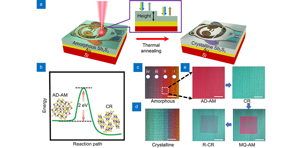
Figure 1.(a) Scheme of a dynamic color display using stepwise FP cavity array based on Sb2S3 switched between amorphous (left column) and crystalline (right column) states. The stepwise FP cavity array consists of air/ Sb2S3/Au with different heights of the Sb2S3 strips. The reflected colors of the structure are associated with the phase and thickness of the Sb2S3. Inset: Schematic of the stepwise FP cavities array. Pixelated Sb2S3 strips of different heights generated by lithography-free fs laser patterning are sandwiched between an air-capping layer and an Au mirror reflector. Resonant modes can be created in the FP cavity, selectively reflecting light with particular colors. (b) Atomic structures: Sb2S3 with the different phases of amorphous and crystalline are shown on enthalpy-order schematic plot. The photo images of the stepwise FP resonators array (c) before crystallizing, (d) after crystallizing the Sb2S3 strips in the cavity. (e) The reversibly switchable photo images of the strip (ii) in figure (c). Scale bar 100 μm.
Figure 3.(a) The measured reflectance spectra (left column) and colors (right column) of the four representative tiles (i–iv) highlighted in Fig. 1(c) during the phase transition of Sb2S3. (b) Color palettes of the structures in amorphous (left column) and crystalline (right column) states as varying the thickness of Sb2S3 from 5 to 30 nm. (c) Raman spectra of the color patch in Fig. 1(c) (ii) for both amorphous and crystalline states, respectively. (d) Color coordinates from the experimentally measured spectra plotted on the CIE 1931 chromaticity figure of the devices as varying the TSbS from 5 to 30 nm.
The high repetition rate fs laser is taken to reversibly convert the state of Sb2S3 film between the amorphous (AM) and crystalline (CR). The parameters of our femtosecond laser pulses are as follows: 800-nm wavelength, 76-MHz repetition rate, and 150-fs pulse width. Particularly, to re-amorphize the CR Sb2S3 strips, the average laser power P1 =35 mW and stage moving velocity v1 = 50 µm s−1 are employed, increasing the local temperature promptly beyond TM= 801 K to melt the Sb2S3. The subsequent fast cooling quenches the melted layer into the AM state. To recrystallize the melting-quenched amorphous (MQ-AM) Sb2S3 film, the laser pulses with a lower laser power of P2 =25 mW and stage moving velocity v2 = 0.5 µm s−1 are used to sustain the material above TG = 543 K but below TM= 801 K. In both cases, the beam waist is around 1 µm.
In Supplementary Fig. S1(a), we schematically present the experimental setup of non-contact microsphere femtosecond laser irradiation. A microsphere is used to focus the high repetition rate fs laser (Mira 900 of Coherent, Inc., 800 nm, 76 MHz) via the objective lens (10×, 0.26 NA). The laser fluence can be tuned by an isolator and half-wave plate. A lens holder can fix the soda-lime glass microsphere with a radius of ~27 μm (SLGMS, Cospheric) and is lined up to a microscope system. The device is placed on a three-dimensional nano-stage with a maximum speed of 5 mm/s, a minimum moving accuracy of 10 nm, and a traveling range of 20 mm (FS-3200P-WE2 series, OptoSigma). The scanning speed of a non-contact microsphere fs laser is 100 μm/s.
Sample measurements
Reflectance spectra
Reflectance spectra of the Sb2S3/ Si3N4/Au stacked layers residing on Si substrate are measured via an FTIR spectrometer (IFS 66 v/s) coupled to a Bruker microscope (Hyperion 2000). The setup records data over the spectrum ranging from 25000 to 9000 cm−1 have a spectral resolution of 1 cm−1. The data are achieved in reflection mode using a 15× objective and Si detector. The scanner velocity is 20 kHz. Interferograms are Fourier transformed, having a Blackman–Harris three-term apodization and a zero-filling factor of 4. The OPUS 6.0 software is used to obtain spectral data.
Refractive index measurement
The complex refractive index of Sb2S3 with both the amorphous and crystalline states is experimentally measured using a variable angle spectroscopic ellipsometry (VASE) spectrometer that is fitted by a Lorentz and Tauc–Lorentz oscillator models. The wavelength of the incidence varies from 400 to 900 nm, and the incident angle is 65°.
Raman spectroscopy
The Raman scattering spectra were collected and analyzed at room temperature using a spectrometer (Horiba iHR550). The structures were excited using a 532 nm solid-state laser. The wavenumber resolution was ≈0.6 cm−1. The laser source beam was focused using a 100× microscope with a 0.2 mm working distance. An air-cooled charge-coupled device (−70 °C) with 1024×256 pixel front-illuminated chip was used to measure the scattering signal dispersed on a grating with 1800 grooves mm−1.
Optical microscopy
To compare the colors of the palette with different phases, the bright-field optical microscopy images of the structure are taken using an Olympus BX51 microscope through a 10× objective lens with a numerical aperture (NA) of 0.3 in a reflection mode of bright-field.
Simulations
The simulated reflectance spectra and the corresponding color patches of simulations in Fig. 3(a) are performed by the Lumerical Solutions software based on the Finite-Different-Time-Domain (FDTD) method. The periodic boundary condition is employed in the x−y plane. In the vertical direction (z-axis), the simulation area is terminated using perfectly matched layer boundary conditions. We normally illuminate the devices by a plane-wave transmitting along the z-axis, and the reflectance is numerically obtained using a power monitor positioned before the structure. A uniform FDTD square mesh (2 nm ×2 nm × 2 nm) is used to decrease the numerical error during the FDTD approximation. Our models employ the Palik permittivity data for Si and Au that considers the losses. The optical constants of the Sb2S3 layer under both structural phases are defined from the VASE measured ones in Fig. 2(b).
Figure 2.(a) Scheme of the reversible phase change of the Sb2S3 film with the various heights integrated with an Au reflector: AD-AM Sb2S3 is first annealed above 543 K to change to CR Sb2S3 using a hot plate. The fs laser pulses (35 mW) are triggered to heat the CR Sb2S3 film above 801 K that re-amorphizes the CR Sb2S3. Subsequent quenching results in the MQ-AM Sb2S3. To recrystallise the MQ-AM Sb2S3, for which a temperature above 543 K but below 801 K is required, the fs laser pulses with lower power (25 mW) are employed. (b) Visible–NIR complex refractive index of 50-nm-thick Sb2S3 laminate at the structural states of the AD-AM (red line), CR (blue line), MQ-AM (orange line), and R-CR (green line), where the refractive index is measured using an ellipsometer over a spectral range of 400 to 900 nm.
A lithography-free and cost-effective technique is employed to make the stepwise FP cavity array. This technique relies on the resonant absorptance of laser light in the cavity. The high resonant light absorptance is achieved through interferometric operating control and absorptance around a crucial coupling condition34. The structural phase change of CPCMs has been used for many tunable photonic applications35. In this work, when antimony trisulfide (Sb2S3) is employed in the FP cavity array, it can be re-amorphized and reversibly crystallized on a sub-nanosecond time scale. Noteworthy, the Sb2S3 post variation to the resonant frequency of a reflector relies upon Sb2S3/Au dual-layered structure over the visible spectrum. Figure 1(a) schematically demonstrates the working mechanism of dynamic color printing. The Sb2S3 films with various heights are patterned onto a 100 nm thick Au mirror residing on a Si substrate using fs laser writing (See top inset of Fig. 1(a)). The fabrication details can be found in the Section Materials and methods. The air layer, stepwise Sb2S3 film, and the Au mirror create a series of asymmetric FP cavities. To offer a palette of colors with a wide range, consecutive resonance tuning of the asymmetric FP cavities is performed by varying laser power. The thickness of each Sb2S3 film varies from TSbS = 5 to 30 nm by changing the laser power, which leads to the pixelated stepwise FP cavity array. The height of the Sb2S3 film is decreased as increasing the power; this produces stepwise Sb2S3 film height changing from 5 to 30 nm in the palette. The power range for the ablation is 0.3~4 mW. The laser repetition rate is frep =1 kHz. The ablation ratio is 34~39 nm per pulse. The minimum ablation depth is ~34 nm. (More details can be found in Section Materials and methods) This stepwise FP cavity array can provide high-contrast and vivid colors with a broad gamut for the amorphous state of Sb2S3. The color of these pixelated palettes can be further dynamically changed by switching the structural phase of Sb2S3 film between amorphous and crystalline. We also include a Si3N4 diffusion barrier between the Au and Sb2S3 film to avoid interlayer diffusion36. Optical lessening within the device is caused by the nontrivial interface reflective phase shifts, leading to resonance absorptance26. Accordingly, our proposed structure possesses resonances, observable as valleys in the reflectance spectra, which produce various colors in the reflected light. The resonant frequencies are associated with the permittivity and the height of the Sb2S3 film. The position of the reflectance valley and the number of permitted modes in the asymmetric FP cavities are dominated by each cavity height.
The interaction of ultrafast laser with the material is mainly concluded as the absorption of photon-induced electronic excitation37. When ultrafast laser irradiates the Sb2S3 film, electrons in the film get on excited by the laser photons. The absorption of photons will generate significant heat in electrons, which can transfer energy to the lattice within picosecond intervals and consequently result in high temperature. When the lattice temperature increases to the melting or even vaporization points, the film will transform from solid to liquid or gas, also the plasma generation38. The ablation produced by ultrafast laser irradiation is affected by processing parameters, including laser power, focal plane offset, scanning direction and speed, and repetition scanning number39. Herein, we achieve the heights of Sb2S3 cavities by changing the laser power. To show the mechanism and process of laser-printed Sb2S3 cavities, a series of results produced at different laser powers are shown in the Supplementary Fig. S2, which are measured by surface profiler (Alpha-Step 500, Tencor inc.). The ablation depth of Sb2S3 film changes from 70 to 110 nm with the increase of laser power from 0.12 to 0.22 mW, as shown in Fig. S2 (a, b). By controlling the laser power, we can ablate different thickness Sb2S3 films and write the color images.
Different from the transition metal oxide PCMs (i.e., VO2), which need constant input power to sustain a structural state40, the amorphous (AM) and crystalline (CR) states of Sb2S3 are stable under room temperature. The energy barrier dividing the two phases (amorphous and crystalline) is 2.0 eV, resulting in the crystallization from the as deposited amorphous (AD-AM) Sb2S3 to the orthorhombic structure at higher temperatures41. This is illustrated by the enthalpy-structural order diagram presented in Fig. 1(b). Although the amorphous structural phase is not as stable as the crystalline phase, the 2.0 eV energy barrier forbids it from crystallizing under room temperature. Crystallization can be obtained by heating Sb2S3 above its glass transition temperature of TG = 543 K long enough to induce crystal creation. Heating is achieved by either electrical or optical pulses that are tens of nanoseconds in duration or by heating up the whole sample. While the crystalline-to-amorphous change, so-called re-amorphization, contains heating Sb2S3 above its melting temperature of TM= 801 K ± 18 K using high-intensity pulses possessing short duration to randomize the atomic arrangement42, 43 and then promptly quenching to “freeze-in” the amorphous state. Herein, we first crystallize the Sb2S3 patch by annealing the FP cavity for 5 min at TG = 543 K on a hotplate in a flowing Ar atmosphere. With the method from ref.32, we reversibly change the state of the Sb2S3 patch from the CR to melting-quenched amorphous (MQ-AM), by melting the crystal lattice and subsequently quenching it into an AM state at a rate of 109 to 1010 K/s44. The cooling down of the film is probably due to the subdiffraction-limited volume of Sb2S3. Since the heated volume is tiny, the structure cannot trap the heat and quenching is achieved within ~13 ns cycle between the fs pulses. The high repetition rate fs laser is taken to reversibly convert the state of Sb2S3 film between the AM and CR (More details can be found in method). Particularly, to re-amorphize the CR Sb2S3 strips, the average laser power P1 =35 mW and stage moving velocity v1 = 50 µm s−1 are employed, increasing the local temperature promptly beyond TM= 801 K to melt the Sb2S3. The subsequent fast cooling quenches the melted layer into the AM state. To recrystallize the MQ-AM Sb2S3 film, the laser pulses with a lower laser power of P2 =25 mW and stage moving velocity v2 = 0.5 µm s−1 are used to sustain the material above TG = 543 K but below TM= 801 K. In both cases, the beam waist is around 1 µm. The laser-induced phase transition of the structure is schematically shown in Fig. 2(a). In Fig. 2(b), it demonstrates the measured complex refractive index of a 50-nm-thick monolithic Sb2S3 layer in the structural phases of AD-AM (red solid line), CR (blue solid line), MQ-AM (red dashed line), and re-crystalline (R-CR, blue dashed line). These dielectric constants are measured in the spectrum ranging from 400 to 900 nm, using a variable angle spectroscopic ellipsometry (VASE) (see methods for details). The variation in the refractive index of Sb2S3 is induced by a bonding switching from predominantly covalent in the amorphous state to resonant bonds in the crystalline state45. The refractive index of Sb2S3 for the crystalline state is much larger than the amorphous state over the visible spectrum from 400 to 900 nm. The variation in the real part of the complex refractive index (N = n + i×k) can achieve the maximum value of Δn ≈ 0.8 at λ= 640 nm. This is higher than that of widely studied typical phase change materials (PCMs) i.e., Ge-Sb-Te28, 46, Ag3In4Sb76Te1747, and Sb2Te348. The extinction coefficient (k) is approximately zero for the amorphous phase at λ > 605 nm. This is crucial since a phase change in Sb2S3 can modulate the absorptance wavelength and the concomitant condition for a photonic resonator's reflectance and absorptance spectra in the visible regime. Such a unique feature implies that the Sb2S3 is a more suitable PCM for non-volatile reconfigurable visible photonics devices. The measured N spectra of the Sb2S3 film with the different structural states are compared. As is seen, the N spectra of AD-AM and CR are close to those of MQ-AM and R-CR. It indicates that the state transition of Sb2S3 is reversible, and the Sb2S3 after the ultrashort-laser-pulse-induced switching resembles the initial phases after hot-plate thermal annealing.
The size of the palette is 400 µm × 400 µm. We present images of the palette with the different structural states of as-deposited amorphous and annealed crystalline. For the AD-AM state, the brilliant colors of the palette cover a broad gamut (Fig. 1(c)). The initial amorphous color can be significantly changed after thermal heating crystallization (Fig. 1(d)). In Fig. 1(e), we showed that the color of strip (ii) in Fig. 1(c) could be reversibly switched. As is seen, the color of strip (ii) can be changed from red to cyan by changing the state of Sb2S3 from AD-AM to CR. The strip (ii) can be reversibly changed from cyan to red by re-amorphising the CR-Sb2S3 strip via fs laser-induced state transition. It can be clearly observed that after fs laser transition, the color of the palette again alters from red (MQ-AM) to cyan (R-CR). The slight color difference between CR and R-CR is likely due to two reasons: a small discrepancy of the crystalline thickness occurs for the different crystallization processes; on the other hand, the fs laser may slightly damage the sample and induce some degradation. In Supplementary Fig. S3, we have shown that by thermally annealing the R-CR FP-cavities at 270 °C for the various durations of 2, 10, and 15 min, the color of device does not significantly change. In Supplementary Fig. S4, we have shown that the color of the palette can cycle between red (MQ-AM) and cyan (R-CR), and the color of each structural state can be maintained well. It is concluded that the Sb2S3 can be re-amorphized and re-crystallised employing the 150 fs laser pulse and offers a vast reversible variation to the visible region. Such a write-erase reversibility of the color variation is crucial for real applications. We find that by designing the resonant frequency of Sb2S3–Au cavity to match the absorptance edge of Sb2S3, the effect of intense interaction can be used to efficiently absorb the 800 nm light in Sb2S3 film, which in turn, permits amorphization. Efficient absorption occurs when the intrinsic absorption of the component layers decreases the light power reflected from the buried interfaces to balance the wave reflected from the top air–Sb2S3 interface. Moreover, any optical phase difference caused by interfacial reflections and path length variations needs to be canceled. The sub-λ/4 thick Sb2S3 laminate presents a strong resonant behavior at visible wavelengths owing to a non –π phase shift at the Au–Sb2S3 interface26. It can cause destructive interaction in the semiconductor layers even with their thickness being an order of magnitude smaller compared to the wavelength of incident light.
To underpin the dynamic pixelated color generation, in Fig. 3 we measure the spectra of their reflectance and Raman signals. The reflectance and color of the representative strips during phase transition are presented in Fig. 3(a). These strips (i−iv) with increasing cavity heights are indicated in Fig. 1(c). As shown in strip (ii) of Fig. 3(a), a valley is observed at λ= 528 nm within a wide reflectance spectrum for the AD-AM state, which corresponds to the pronounced FP resonance originating from the cavity created between the air capping layer and the Au reflection mirror. It leads to a red color (see Figs. 1(c) and 3(a)). The resonant dip of reflectance spectrum red-shifts by ~100 nm from λ1= 528 nm to λ2= 628 nm with a decreasing full width at half maximum (FWHM) from 230 nm to 160 nm as switching the state of Sb2S3 from AD-AM (green solid line) to CR (green dot line). Such drastic modulation of the resonance behavior through phase change renders sharp transformations between the red and cyan states (see Figs. 1(d) and 3(a)). The red-shift to the spectra is directly owing to the intrinsic absorptance edge of Sb2S3 narrowing from 2.0 to 1.7 eV. The air–Sb2S3–Au trilayered structure is designed to possess the resonant wavelengths close to this absorption edge, which improves the effect of the absorptance edge switching ON/OFF the resonance frequency, hence offering the vast variation in reflection color. Namely, as switching the state of Sb2S3 between amorphous and crystalline, a profound change occurs in the refractive index of Sb2S3, leading to a color variation. Yet, the FP cavity with the CR state is slightly more absorbing than the AD-AM state, which causes a broader resonance. As increasing the height of Sb2S3 film for the AD-AM state, the dip reflectance wavelength redshifts to longer wavelengths (see Fig. 3(a) (i−iv)). The reflectance dip appears at the shorter wavelengths relating to a FP resonance, which changes the spectral profile to generate color with a broad gamut. Notably, the FP cavity mode varies from 400 to 750 nm by increasing the thickness of the Sb2S3 strip from TSbS = 5 to 30 nm. Meanwhile, the state change of the Sb2S3 strip with a fixed thickness red-shift the resonator’s frequency, offering a strong variation in reflected color. The capability of radically engineering the resonance wavelength and largely modifying the spectral profiles by varying the effective cavity heights through phase change of Sb2S3 indicates an efficient solution to obtain dynamic color displays. The cycle endurance of color change is also important to explore its technical applications. It is expected to be relatively large since its composition is similar to the eutectic compound48. Thereby, structural state separation is less likely. Yet, both the Sb2S3 layer and Au reflector exhibit the high absorption in the visible spectrum, the efficiency and bandwidth of the FP cavity are low and wide, presenting small quality (Q-) factor49, 50. Moreover, the reflectance at the interface between air and Sb2S3 is weak which makes the bandwidth even wider51. Figure 3(b) presents the measured colors of the rewritable device as changing the thickness of Sb2S3 from 5 to 30 nm. A series of colors for the amorphous state, including yellow, orange, purple, red, blue and cyan can be observed. By thermally annealing the devices at 270 °C for 2 min, the corresponding crystalline samples are inhomogeneous and perform a color deviation. In Fig. 3(c), the Raman spectra of the color strip in Fig. 1(c) (ii) further indicate the phase transition between amorphous and crystalline in Sb2S3. The spectrum of the amorphous Sb2S3 film possesses two wide bands at ~290 and ~100 cm−1, shown in a red solid line. These bands are associated with the vibrational Sb─Sb bonds in the SbS3 pyramids and S2Sb-SbS2 structural units, respectively52, 53. For the thermally annealed sample, the band at 290 cm−1 is split into two sub-bands, and the band at ~100 cm−1 is further split into many small peaks (shown in the blue solid line), which is consistent with the Raman characteristics of crystalline Sb2S3. These Raman spectra confirm that the observed color change in Fig. 1(c) (ii) is driven by the phase transition of Sb2S3 between amorphous and crystalline. In order to quantify the color distributions for both amorphous and crystalline states, the corresponding color points are figured on the CIE (International Commission on Illumination) chromaticity diagram, as presented in Fig. 3(d). The color difference between amorphous and crystalline states is considerable. Furthermore, the devices based on both the amorphous and crystalline phases occupy a considerable gamut within the color space of sRGB (standard Red Green and Blue).
To confirm that the color variation in Fig. 3 is owing to the dielectric constant variation afforded by both amorphous-crystalline state transition and thickness alternation, the reflectance spectra and colors of these patches (i−iv) are simulated, as shown in Fig. 4. A commercial Lumerical Solutions software relied upon the finite difference time-domain (FDTD) method is performed to numerically solve Maxwell’s equations for the structures. In the simulation, the dielectric constant of the Sb2S3 layer with the various structural phases is determined by the measured data in Supplementary Fig. S2(b). The permittivities of Au and silicon (Si) substrate are taken from Palik54, 55. The Si3N4 is defined as a lossless dielectric with a refractive index of NSiN = 256. A specific description of the model is presented in the method. As is seen, the simulations match the measurements well in both reflectance spectra and colors, which confirms that the refractive index variation caused by state change has produced the color variations in the device. The tiny variation between measured and numerical data stems from the existence of surface roughness, fabrication imperfections, native oxides, and a finite acceptance angle of 0.3 NA microscope objectives57. It also indicates that a broad gamut of colors can be obtained by changing both the height and structural states of the Sb2S3 strip. The thicknesses of Sb2S3 (TSbS) were theoretically deduced58, by considering incident light from air onto a Sb2S3, Si3N4, Au, and Si four-layer system. In the model, the thicknesses of Si3N4 and Au films are 5 nm and 100 nm, respectively. The reflectances of stacked layer with the different TSbS are numerically calculated by using the finite difference time-domain (FDTD) method and compared with the measured reflectance. The TSbS can be determined if root-mean-square error (RMSE) is minimum59:
Figure 4.The simulated (a) reflectance spectra and (b) color palettes of the devices in structural states of amorphous and crystalline for the different thicknesses of Sb2S3 of TSbS = 10, 15, 20, and 30 nm, corresponding to the color tiles (i−iv) shown in Fig. 1(c).
where m represents the number of sampling points in the visible spectrum from 400 nm to 900 nm and is set as m = 501, Rexp the measured reflectance, and Rfit the calculated reflectance60.
To illustrate the possibility of making arbitrary dynamic microprints, a color display is fabricated using “Bing Dwen Dwen” from the Beijing Winter Olympics 2022 mascot as a design blueprint. A database is first formed using the palette colors in Fig. 3(b). This database contains library values of Red−Green−Blue (RGB) and laser power information. We use the femtosecond laser pulses generated from the commercial direct laser printing system to thin the Sb2S3 film and write the color images. The generated color is associated with the dip resonant wavelength of the Sb2S3–Au cavity, where the resonant wavelength is dependent on the thickness of Sb2S3 film and the thickness can be engineered using laser power. By adjusting the power of laser irradiation, various colors can be processed in different parts of Bing Dwen Dwen (blue leg, orange right hand, light red left hand, and yellow face). In the left column of Fig. 5(a), we present the scanning electron microscope (SEM) image of the fabricated display. In the middle and right columns of Fig. 5(a), we experimentally perform the dynamic color display using snapshot pictures of the device for AD-AM and CR states, respectively. We crystallize the AD-AM Sb2S3 by thermally annealing the device on a hotplate, where an abrupt color variation (from blue leg to cyan leg; from orange right hand to purple right hand; from light red left hand to light purple left hand) occurs in the printing of “Bing Dwen Dwen”. In addition, one colorful “DUT” image is printed on the Si wafer shown in Fig. 5(b), with a large color variation, which includes yellow, red, purple, blue, and cyan. In the middle and right columns of Fig. 5(b) we present images of the “DUT” with the different structural states of as-deposited amorphous (AD-AM) and annealed crystalline (CR). This scenario confirms the observed dynamic structural state-altering results with the color changes. This is a viable and scalable approach for tunable modern devices with nanometre precision on large-area substrates.
Figure 5.(a) The SEM picture of the fabricated “Bing Dwen Dwen” display (left column) and optical micrographs of the “Bing Dwen Dwen” (middle column) before crystallizing, (right) after crystallizing the Sb2S3 in the device. (b) The SEM picture of the fabricated “DUT” display (left column) and optical micrographs of the “DUT” (middle column) before crystallizing, (right) after crystallizing the Sb2S3 in the device. Scale bar 200 μm.
The laser processing technique depending upon strong light-matter interaction has broadly applied in manufacturing micro/nanostructures37, 61-64. Traditional laser processing is based on the intense energy density in a focused beam, which, in combination with an ultrafast laser pulse (fs to ps), restrain the laser-induced heating region spatially65, 66. The restrained thermal dispersal to the surroundings improves the spatial resolution. Although complex micro/nanostructures can be precisely realized through ultrashort laser direct writing67, the formidable challenge of ultrashort laser processing to produce ultrasmall, subwavelength, features is the optical diffraction limit. In Supplementary Fig. S1, we have experimentally demonstrated that an fs laser integrated with a non-contact microsphere can be employed for super-resolution nanofabrication by laser ablation. Such a technique may have a potential for obtaining a structural color display with nm- resolution.
Conclusions
In summary, we have demonstrated a strategy for generating ultrathin, solid-state, super-high-resolution, and dynamic color displays using Sb2S3-based pixelated FP cavities. Such a color-displaying device exploits the drastic variation of refractive index induced by the phase transition in Sb2S3. By controlling the laser intensity of fs laser pulses, a reversible phase transition between amorphous and crystalline is verified by measuring optical constants, Raman spectra, and reflectance spectra. With the fs laser pulses and thermal heating, the interference colors can be cycled backward and forward by changing the structural phases of the Sb2S3. Moreover, the fs laser pulses are used to print the different color pictures in the identical area of the device with a sub-diffraction resolution by unique non-volatile and reversible properties of phase transition in Sb2S3. Herein, sub-50 nm nano-lines are successfully fabricated on 30-nm thick Sb2S3 laminate via the microsphere fs laser irradiation in far field and ambient air. Our data explores the promising potential of Sb2S3 for the ultrafast and flexible fabrication of reconfigurable photonic devices. We anticipate that this proposed sub-diffraction and ultrathin rewritable color printing method based on the Sb2S3 are useful for next-generation high-resolution optical encryption and color display devices.