
James Garofolo, Ben Wu. Photonic analog signal processing and neuromorphic computing [Invited][J]. Chinese Optics Letters, 2024, 22(3): 032501
- Chinese Optics Letters
- Vol. 22, Issue 3, 032501 (2024)
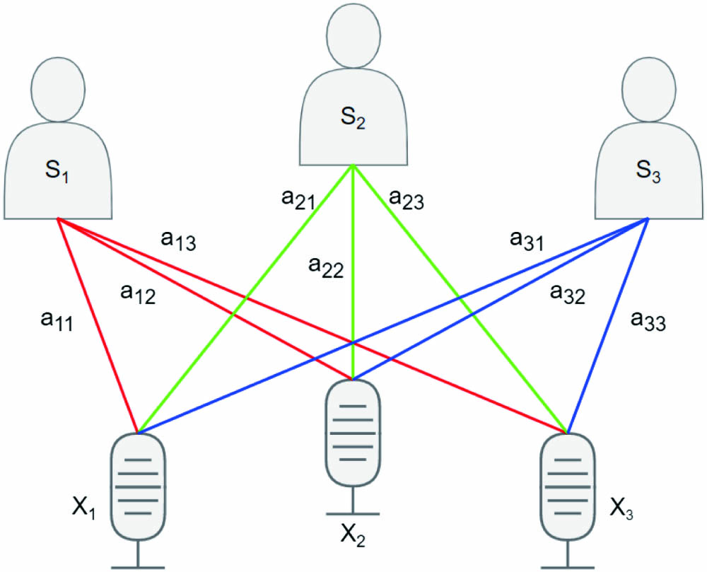
Fig. 1. Diagram illustrating the cocktail party problem with 3 transmitters and 3 receivers.
![Schematic of a common single-output photonic BSS circuit. TD, tunable delay; AM, amplitude modulator; TA, tunable attenuator; PD, photodiode; ADC, analog-to-digital converter[42].](/richHtml/col/2024/22/3/032501/img_002.jpg)
Fig. 2. Schematic of a common single-output photonic BSS circuit. TD, tunable delay; AM, amplitude modulator; TA, tunable attenuator; PD, photodiode; ADC, analog-to-digital converter[42].
Fig. 3. Schematic of an ASE-based stealth communication system[9].
Fig. 4. Schematic of a chaos-based free-space optical stealth communication system[48].
Fig. 5. Micrograph of a 4-ring single-pole through-drop resonator weight bank with schematics showing control, input, and output signals[56].
Fig. 6. Schematic of a through-drop resonator based photonic neuromorphic circuit[17].
Fig. 7. Block diagram of a scalable digital electronic and analog photonic neuromorphic processor[59].
Fig. 8. Schematic of a WDM-compatible GST-based attenuator bank[22].
|
Table 1. Comparison of Power, Performance, and Area Metrics
|
Table 2. Comparison of Accuracies and Effective Precisions

Set citation alerts for the article
Please enter your email address
© Copyright 2018-2021 | Chinese Laser Press. All Rights Reserved 沪ICP备15018463号-20