 AI Video Guide
  AI Picture Guide
 AI One Sentence

James Garofolo, Ben Wu, "Photonic analog signal processing and neuromorphic computing [Invited]," Chin. Opt. Lett. 22, 032501 (2024)
- Chinese Optics Letters
- Vol. 22, Issue 3, 032501 (2024)
Note: This section is automatically generated by AI . The website and platform operators shall not be liable for any commercial or legal consequences arising from your use of AI generated content on this website. Please be aware of this.
Abstract
1. Introduction
Photonic circuits are a tool that enables a wide variety of applications in the domain of analog signal processing. The low power consumption and high bandwidth allow for the implementation of operations from basic arithmetic to frequency domain manipulation at speeds and efficiencies that their electrical counterparts are unable to approach[1]. This high bandwidth also enables massively parallelized computations through the use of wavelength-division multiplexing (WDM). Their analog nature allows for signal processing in continuous time, and reduces the cost, memory requirements, and precision loss resulting from the need to digitize massive amounts of data. Not only are these advantages for applications involving optical signals, such as optical fiber or free space optical communication[2–13], but they also show promise when applied to computation in general[14–24].
In recent years, there has been a push toward implementing physical layer solutions to problems that are currently handled in software. The rapid reconfigurability and deterministic operation of digital electronics make it appealing as a foundation for solving any engineering problem, but it is not always the optimal solution. The discrete nature of computers forces quantization, which adds a small amount of noise to the measured signals. It also forces discretization of incoming signals[25], which can drive up the price of circuitry in high-frequency applications and add latency to systems that may need to operate in real time. Furthermore, in comparison to photonic circuits, digital computers have drastically lower bandwidth, meaning that some applications will force space-consuming and power-hungry parallelism to meet performance requirements, while some that are not easily parallelizable become functionally impossible after a certain threshold for speed requirements is crossed. Converting solutions that are sub-optimally implemented by computers to the physical layer removes these limitations and leverages the unique advantages of the circuit paradigm to make elegant work of complex, difficult, and performance-sensitive programming tasks. In this review, we will address some of these problems that photonic circuitry is uniquely qualified to solve.
Photonic circuits achieve many useful effects through the strategic splitting and combining of signals. Linear mixing through coupling or over-air transmission provides an avenue for technologies like optical steganography, which aims to hide communication signals by combining them with noise[6,26]. This phenomenon also causes interference in communication lines, prompting the exploration of using photonic blind-source separation to recover signals as they were before mixing[2,5]. Combining these linear operations with nonlinearities caused by excitable lasers[27] or resonator-based modulators[28] allows for the creation of photonic neural networks, effectively allowing any function to be created so long as the hardware requirements can be met[15]. All of these capabilities show potential for improving high-speed communication systems, as they require throughputs that would overwhelm most analog electrical circuitry, and drive up the price of digital signal processing techniques through increasingly high-speed analog-to-digital converters. They also show promise for accelerating general computation, as many of these devices are capable of being integrated into silicon wafers and used as application-specific co-processors in tandem with digital and analog electrical circuitry[18].
Sign up for Chinese Optics Letters TOC. Get the latest issue of Chinese Optics Letters delivered right to you!Sign up now
Photonic blind-source separation is a technique that uses photonic circuits to manage interference in wireless communication systems[2–5], free-space optical communication systems[4], and optics-based sensor technologies[29,30]. It takes advantage of the rich amplitude information present in multi-input-multi-output signal processing systems to separate signals that exist in the same electromagnetic bandwidth, circumventing the limitations of traditional frequency filtration and multiplexing techniques. Digital blind-source separation was first proposed in 1991 in Ref. [31], alongside independent component analysis, which is a dimensionality reduction technique invented for this purpose. Photonic blind-source separation was first demonstrated in 2018[2], where the high throughput of photonic arithmetic circuitry was leveraged to separate communication band RF signals in real time. Since then, several techniques for improving the method have been explored, such as sub-Nyquist optical pulse sampling[32], genetic algorithms for PC/IC searching[33], and hybrid signal domain systems for increasing the likelihood of separability[4,5].
Optical steganography is another technique that is built upon the advantages of photonic signal processing circuits. This technique aims to disguise sensitive communications as system noise, preventing eavesdroppers from interpreting, recording, or potentially even noticing them[6–12]. It takes advantage of inexpensive, easily implemented spectral manipulations to hide the sensitive signals, acting as a hardware keyspace that is very difficult to search as an unintended recipient[6,9,26]. The technique was first introduced in 2009 in Ref. [6], where dispersive elements were used to hide a narrow band communication signal in a massively multiplexed communication network. Since then, other techniques for performing optical steganography have been introduced, including noise based stealth communication[9,26] and optical phase-mask encryption[11].
Photonic neuromorphic computing is a field that aims to leverage the advantages of analog photonic circuits for high-performance computing tasks. In particular, it leverages the high speed, wavelength-division parallelism, and low power consumption of photonic arithmetic operations to accelerate the calculations that make up artificial neural networks[14,16–24,27,28,34–37]. This enables simple yet powerful networks to solve complex tasks at the speed light transmission[13]. It also promises to efficiently accelerate deeper neural network inferences to speeds that rival modern GPU technology[19]. A pioneering work of photonic neuromorphic computing was introduced in 2009 in Ref. [14], where it used photonic spike processing to perform the operations of a spiking neural network. Since then, multiple techniques have been made to improve upon this design, including tunable weight banks made from interferometers[14,35], tunable resonators[15–17], or phase-change elements[22–24,34], as well as a variety of output designs including all-optical thresholders[22,23], electro-optical nonlinear laser gates[28,36], and electrical sampling and reproduction circuitry[18,19,24]. Today, it is showing particular promise in the fields of high speed neural signal processing[13,37] and machine vision acceleration[19–24].
In this paper, we review the principles and emerging developments in each of these sub-fields of computational photonics. In Section 2, we review methods of photonic blind-source separation and their applications in interference cancellation and multiplexing. In Section 3, we review methods of physical layer steganography, and analyze them in terms of signal quality, security, data rate, and public channel coexistence. In Section 4, we introduce the principles of photonic neuromorphic computing and discuss both through-drop resonator and phase-change material methods in their respective subsections. We will also analyze different hardware architectures that are native to each technology and the software architectures for which they are most advantageous.
2. Photonic Blind-Source Separation
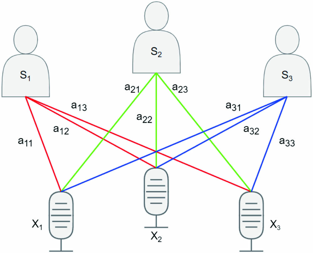
Blind source separation (BSS) is a technique that aims to solve the problem of separating interference signals from signals of interest without knowing anything about the nature of either signal[2–4,31,38,39]. This is commonly referred to as the “Cocktail Party Problem,” which is illustrated in Fig. 1. In this scenario, three transmitters (represented by humans speaking at a cocktail party) are communicating with three receivers (represented by microphones). Each receiver receives a scaled copy of each message, additively combined together to form a single signal. This forms what is referred to as a “multi-input-multi-output” (MIMO) system, where the three intended recipients have access to all three received messages and are tasked with interpreting their intended message as it exists in the mixtures[39]. Humans are able to do this naturally, taking advantage of the directionality of their ears to localize and attend to their source of interest while ignoring other conversations, which can be considered “interference” in this context. This human intuition has led to an emergence of sciences aimed toward using amplitude information resulting from spatially separated sources and receivers to manage electromagnetic signal-signal interference that cannot be managed traditionally.
![]()
Figure 1.Diagram illustrating the cocktail party problem with 3 transmitters and 3 receivers.
An MIMO system with two inputs and two outputs can be mathematically described as the following[2,32]:
The condition number of a singular matrix is infinite. Finite values for the condition number quantify the sensitivity of the inversion to inexact matrix elements that can be caused by chaotic factors like statistical variance, floating point error, or device non-idealities[4,40]. Larger condition numbers describe more sensitive systems, for which the blind-source separation algorithm will generally perform worse. Smaller condition numbers describe matrices that can tolerate more inaccuracy in their inversion, resulting in a more successful de-mixing. In practice, mixes tend to be well conditioned when coefficients corresponding to a given transmitted signal are different for different received signals, or, more formally,
This condition can be met by sufficiently spatially separating the transmitters and receivers, such that the transmitted signals take drastically differing paths to each receiver. This requirement makes implementation of BSS systems in mobile devices and smaller embedded systems difficult, as the spacing of receiver antennae is constrained[4].
The problem of BSS requires that the mixing matrix be treated as an unknown, and it tasks the system with determining the elements of the de-mixing matrix using only the information present in the
In the two-signal case, the unit vector in the direction of the first projection axis can be described in terms of its angle with respect to the
By projecting the signals onto this new axis, the resulting output signal will be shown to have some variance about the zero point. This variance can be quantified by the second-order moment of the signal across all available time. This quantity can be expressed as the following:
Once the process of PCA is finished, the projections could be taken as is[3]. However, the optimal projection axes are not necessarily orthogonal, and PCA assumes that they are. In order to allow for the projection axes to take on non-orthogonal positions, which will provide a closer fit with less interference, the PCs must be used to perform ICA. The key step to ICA is called “whitening,” wherein each of the signals is rescaled such that they all have the same variance, with the intuition being that this will move the optimal projection axes into orthogonal positions. The unit vector in the direction of this new projection axis can be mathematically described as
This moment can be minimized using the same process as the second-order moment, resulting in a new rotation angle
To implement this de-mixing in the physical layer, the received signals need to be aligned in time, scaled by the elements of the row of the de-mixing matrix that corresponds with the signal of interest, and then additively combined to cancel the interference signal out. A typical schematic for a system that performs these operations with photonic circuit elements is shown in Fig. 2. This diagram is intended to receive RF signals through antennae
![]()
Figure 2.Schematic of a common single-output photonic BSS circuit. TD, tunable delay; AM, amplitude modulator; TA, tunable attenuator; PD, photodiode; ADC, analog-to-digital converter[
The success of these systems is typically evaluated using the signal-to-interference and noise-ratio (SINR) of the signal of interest after cancellation. This can be calculated as the power of the signal of interest divided by that of the difference between the signal of interest and the resulting separated signal. If the experiment is simulated, then the denominator should also be made to include the variance of any noise the signals are likely to encounter along their optical path. In a previous experiment, we found that the SINR of a separation attempt in dB is loosely inversely correlated to the condition number of the mixing matrix that is being used[4]. This means that there is a fairly wide range of tolerance for ill-conditioned matrices that are separable to a degree that enables error-free communication. Though this range is not infinite, there are a number of techniques that have been developed to combat this vulnerability, such as hybrid RF and optical systems that ensure well-conditioned mixes by guaranteeing that one of the cross-channels has a mixing matrix coefficient of zero[4].
Some key advantages of this technology lie in the frequency independence of the separation algorithm. Because spectral methods are not used for the separation process, signals can safely exist in the same bandwidth as each other. This enables a type of space-division multiplexing that does not require separate transmission mediums for each signal[45] and shows potential for increasing the capacity of fiber optic communication networks[38,39,42]. In addition, because the algorithm makes no attempt to digitally reproduce the signals being analyzed, the sampling circuitry is capable of working well below the Nyquist sampling limit[2,3]. This allows systems to use much simpler and cost-effective sampling circuitry while working on much higher data rates than that traditional digital signal processing methods are capable of handling[32].
One interesting application for this technology is the pursuit of RF spectrum coexistence in broadcasting systems. This deals with the problem of long-range RF transmitters strongly interfering with nearby unintended recipients along the path to the further intended receiver that is out of the line-of-sight. In a previous work[5], we proposed solving this problem by having the transmitter generate a copy of the transmitted signal with a free-space optical transmitter. This would allow unintended receivers within the line-of-sight to use photonic BSS to cancel the transmitted signal out of what they receive so that their signal of interest can present uncorrupted. This method is also immune to the problem of ill-conditioned mixes because the signal of interest exists only as an RF signal. This forces the cross-channel coefficient for the signal of interest to go to zero, which prevents the condition number of the matrix from approaching infinity.
3. Optical Steganography
Steganography is a method of ensuring communication security that focuses on keeping decryption attempts from occurring, rather than focusing on stopping them from succeeding[6–11,26,46]. While optical cryptography is a powerful tool for protecting the encrypted data[47], the presence of a digital communication signal that needs to be decrypted can be enough to prompt an attacker to record the signal and attempt to decrypt the message digitally through brute force[9]. To avoid this, the signal can be disguised as something that would appear inconspicuous to a potential attacker, preventing any decryption attempt from being made in the first place. A helpful example is file-type based steganography, which attempts to hide sensitive digital data in the least significant bits of the pixel data in image files or the amplitude data in audio files[46]. The less important a signal appears to a potential eavesdropper, the more theoretically secure the contained signal will be, so the natural ideal condition is to use the physical layer to generate a signal that does not appear to be a communication signal at all.
Optical steganography is the practice of using photonic circuits to perform steganography in the physical layer. The sensitive signal in this practice is typically disguised as some form of system noise, which an eavesdropper would likely attribute to the sources of visible non-sensitive signals and discard[6,9,26]. This is a strong disguise to use, as it does not outwardly portray that information is present in the stealth channel at all, effectively requiring prior knowledge of the technique to prompt an attempt to recover the hidden signal. This is also preferable for the goal of increasing communication speeds, as digital techniques like file-type based steganography require the deployment of a large portion of data space to make the signal seem inconspicuous. While this tradeoff between channel capacity and information security is, in some ways, inherent to the nature of stealth communication, photonic circuits have been demonstrated to present a wide variety of opportunities for increasing the security of a communication system that involve little to no channel capacity waste[6–11,26]. In addition, the photonic circuits that perform these tasks almost always involve some non-standard receiver architecture, without which the signals tend not to appear to carry information at all. This requirement effectively acts as a massive key space that secures the information, and the relatively high sensitivity and low variability of certain components protect strongly against brute force attacks even if an attacker can guess the general architecture of a stealth receiver[6,9,26].
One method of performing optical steganography is through the use of intentionally introduced wavelength dispersion. This method is unique to narrow band WDM channels, as it relies on spectral filtering to separate the public channel from the private channel before detection[6–8]. Passing signals through a dispersing element widens them in time and suppresses their amplitude, making them appear insignificant in comparison to normal communication signals. To recover the signal, the signal can be re-dispersed in the equal and opposite manner, returning the signal to the high amplitude communication signal it was generated as. A circuit that accomplishes this method of optical stealth communication is shown in Ref. [7]. This circuit uses a pair of chirped fiber Bragg gratings (CFBGs) in combination with optical circulators to disperse the signals. This has the added benefit of spectrally filtering the incoming signals, such that the wavelengths of interest are reflected back through to the output port of the circulator, while the remaining wavelengths are passed through to an optical power sink. This method is very time and material efficient for this reason, as no additional filtration hardware or post-processing algorithms are necessary to recover the stealth signal from the mix with public access signals.
One advantage of dispersion-based steganography methods is that they are effective for a variety of different modulation techniques, making them very easy to include in existing optical communication systems. In addition, compatibility with any modulation format means that all axes that are used to encode information are usable, so there is no sacrifice of channel capacity required to gain the promised security so long as the required signal quality characteristics are met. That said, this method only renders signals undetectable in time and does not effectively change the spectral content. This leaves the method vulnerable to detection by analyzing the optical spectrum present in the transmission line. This vulnerability can be mitigated by implementing this steganography method in a system that uses a type of orthogonal signal multiplexing in the same spectral region, such as code-division multiple access (CDMA). This ensures that the optical spectrum of the public channel will appear inconspicuous, as the amount of power contributed by the stealth channel to the wavelength region of interest will be relatively negligible in comparison to the total power in that region. In the event of the stealth channel’s detection, a potential eavesdropper may still be deterred by the large potential key space that is the dispersion reversing CFBG’s grating pattern and the difficulty involved in searching that key space manually.
Another method of securing optical communications is through the use of noise carrier signals[9–11,26]. These signals are typically the product of the amplified spontaneous emission (ASE) noise caused by erbium-doped fiber amplifiers (EDFAs). Because of their wide spectral content, the coherence length of these signals can be on the order of hundreds of micrometers. Noise-based stealth communication systems take advantage of this small coherence length by using a specific length of optical delay to intentionally create an incoherent combination of phase-modulated signals and unmodulated ASE noise. This gives the resulting communication signal the time and frequency domain appearance of noise that is inherent to fiber optical communication systems, and it will continue to present as such even in the event that a standard coherence detector is used to demodulate the signal. Coherent detection of the signals will occur only when the difference in the optical delay between the two paths of the coherence detector is equal to that of the transmitter, at which point the output signal will appear as a combination of the stealth signal and beating noise caused by the incoherent interference of the unmatched paths. A circuit that implements this method of stealth communication is shown in Fig. 3. In order to prevent the detection of encoded information, this system elects to relinquish control over the amplitude of the transmitted signal. This does decrease the information capacity of the channel, though this comes with the benefit of leaving the transmitted information functionally invisible in both time and frequency unless the required demodulating technique is being used. The key space created by varying the optical path lengths is very large, considering the high precision required for a sufficiently matched receiver, though it is slightly more vulnerable to brute force attacks due to the commercial availability of tunable optical delay lines. This risk can be compensated for by the addition of high frequency random phase mask encryption[11] or by combining the modulation technique with dispersion-based steganography to create an orthogonal 2-dimensional key space[10].
![]()
Figure 3.Schematic of an ASE-based stealth communication system[
Because this method of steganography involves a unique modulation technique, it is important to perform a noise analysis of the technique to ensure an acceptable rate of error[12]. The signal-to-noise ratio (SNR) of the system shown in Fig. 3 can be modeled as
This equation shows that the SNR increases with the ASE noise power, saturating as the beating noise begins to dominate the other two types of noise. Increasing
This is a valuable result, as it does not motivate the designer of the stealth transmitter to add arbitrarily high amplitude noise to the system unnecessarily. It also demonstrates that the SNR can be controlled simply by changing the ratio of the optical bandwidth of the carrier to the electrical bandwidth of the photodiode, which should not affect the security of the transmitted information at all[12].
The benefits of ASE-based optical steganography are most readily apparent in the application of LiFi systems, which attempt to use visible light to transmit communication data[48]. For this application, as well as other free-space optical (FSO) communication techniques, wideband light sources are uniquely preferable. This is due in part to the fact that light cannot penetrate opaque materials, so transmitters must be inexpensive enough to place in every room of a building[49]. LiFi also demonstrates a particular demand for wideband sources, as it is intended to use the light sources for illumination as well as communication[50]. For these reasons, LiFi systems and FSO broadcasting systems are both well suited for being secured via optical steganography. A diagram of a circuit that implements optical steganography in an FSO communication system is shown in Fig. 4. This circuit provides a secure foundation upon which FSO broadcasting systems are built for public use, as a potential eavesdropper may not assume any data transfer is occurring at all when attempting to observe the stealth channel without the proper receiver.
![]()
Figure 4.Schematic of a chaos-based free-space optical stealth communication system[
One drawback of ASE-based steganography is that it has a low rate of error-free communication due to the inherent prevalence of beating noise in the homodyne detection. Experimental results demonstrate stable communication requiring a bit rate for on-off-keying as low as 1 GB/s[51]. Methods of generating chaos through other forms of optical circuit noise have been observed to improve the data rate of stealth communication systems, but at the expense of security, stability or implementation complexity[52]. To eliminate the tradeoff, ASE noise can be generated externally and then leveraged to corrupt a non-chaotic signal in a manner that is uniquely reversible. Common methods for doing this involve phase-to-amplitude noise conversion, which can be added to and removed from a signal using fiber Bragg gratings. This eliminates the need for beating noise at the receiver while still giving the data the time and frequency domain appearance of noise[53].
Other non-standard carriers have been explored for optical steganography as well. One carrier of particular promise is a frequency comb, where independent copies of the baseband signal are modulated onto each tone and then transmitted simultaneously. This enables multi-homodyne detection, where the signal strength is scaled quadratically with the number of carrier tones while independently accumulated noise is only scaled linearly. This superlinear scaling of signal power allows the user to transmit power with an irrecoverable optical SNR, both encrypting the signal and giving it the spectral shape of pure noise. This, combined with a spectral phase mask to hide the time-domain waveform, provides security and steganography with data rates as high as 40 GB/s while being completely agnostic to modulation format[54]. These characteristics make this technique favorable for providing moderate security in applications where data rate is of high importance.
Another non-standard carrier method is to use the bias port of a Mach–Zehnder modulator to use public data as a subcarrier for the private signal. By leveraging high-precision tuning methods, the bias point of the modulator can be switched between two very close values, changing the shape of the public waveform by an amount that is imperceptible to the human eye. By circularly shifting the sampled vector into a 2-dimensional grayscale image, a convolutional neural network can then examine the data shape and classify which bias point was used to transmit the data. This method of transmission is significantly slower, with experiments showing a data rate of 195 MB/s, but it comes with the benefit of having the data be almost completely imperceptible without prior knowledge of its existence[55]. What is more, because MZM bias does not need to be a precise parameter in traditional on-off-keying systems, any perceivable variation could be explained by device non-idealities in the communication circuit, further encouraging a potential eavesdropper to discard the data as non-sensitive. It does not provide analog cryptography by itself, but nothing about the method prevents cryptography from being viable in combination with it. This makes the method favorable for applications where data rate is not very important but where security is paramount.
4. Photonic Neural Networks
As with any analog computing paradigm, a promising application that pushes computational photonic circuits to their limit is neuromorphic computing. This field involves the implementation of analog circuits that perform the calculations that artificial neural networks perform in software. This has the advantage of enabling processing speeds fast enough to meet the throughput demand of real-time applications. In addition, the device interactions of analog computational circuits consume far less power than the equivalent series of digital operations on average, meaning that the paradigm illustrates potential for reducing the environmental impact of server computing companies as well. In this section, we will introduce a variety of neuromorphic photonic circuits and discuss the applications for which they show particular promise.
The pioneering work of designing a photonic neural network (PNN) was developed by the Lightwave Communications Research Labs from Princeton University in 2009[14]. It used a combination of optical combiners, tunable attenuators, Mach–Zender interferometers, integrating silicon optical amplifiers, and optical thresholders to make a photonic spike processor that could operate at communication speeds. While this design was a critical step forward for the technology, it suffered from a number of shortcomings that made it difficult to generalize to the greater field of neural inference acceleration, namely, the circuit size per input was far too high in this form. The use of MZIs for input modulation prohibits the use of wavelength-division multiplexing for a large portion of the circuit, making it near impossible to fabricate at a scale that would provide a useful amount of model complexity. In addition, the all-optical nature of this design posed challenges with implementing larger networks, in that the next hidden layer of neurons in the network would necessarily need to be a separate circuit, thus rendering perceptrons with numerous hidden layers impossible to represent in a cost-effective manner.
Further works in photonic neuromorphic computing have been focused on solving this problem of implementing wider and deeper neural networks in hardware[15,18,19,22]. While output technology, output signal domain, and input/output signal behavior are all of some consequence to the performance of a PNN, by far the most promising area for improvement is the method of implementing weighted addition. Improvements to these technologies promise to better meet the demand for increased fan-in, as well as to improve the precision of the computation and the rate at which inferences can be made[19,43]. Two types of architecture have shown particular promise for this application: through-drop resonator methods, which leverage the thermally variable spectral response of micro-ring resonators to variably weigh signals of a specific wavelength, and phase-change material methods, which change the attenuation constant of a waveguide over length to variably weigh any wavelength. In Subsections 4.1 and 4.2, we will review the working principles, key innovations, and relevant applications of through-drop resonator methods and phase-change material methods, respectively. In Subsection 4.3, we will compare the tradeoffs associated with each methods and review supporting advancements that benefit them both.
4.1. Through-drop resonator methods
In order to increase the fan-in of these circuits, the weight implementation needed to be changed to a WDM-compatible variable attenuator. Doing so would allow the arithmetic circuits to span the footprint of only one waveguide, rather than requiring one circuit for every input signal. The simplest way to achieve this function is by abusing the gradual wavelength response of variable wavelength resonators to specifically target and weigh individual inputs. This can be done using mirco-ring resonators (MRRs), which can be made wavelength-tunable by way of heating the ring to change its refractive index[16]. This method reduces the footprint of the circuit considerably, with the new bottleneck being found in the size requirements of the resonators and the spacing of each resonator’s on-resonance point in the optical spectrum, rather than in the number of parallel waveguides that can be fabricated[15].
An example of a photonic circuit that takes advantage of these devices is shown in Fig. 5. As this figure illustrates, these MRRs can be cascaded into one another, resulting in a 4-port device with variable transfer curves. Because single-pole resonator circuits like this one interfere with one another in a resonator-like fashion[57], the port diagonal to the input port effectively never carries optical power, leaving three ports of significant interest to designers. The port that is directly connected to the input port is called the “THRU” or “THROUGH” port because all wavelengths of light pass through this port except for those which the resonator bank are designed to block. The transfer curve from the input port to the through port of one of these resonators can be described using the following equation[19]:
![]()
Figure 5.Micrograph of a 4-ring single-pole through-drop resonator weight bank with schematics showing control, input, and output signals[
The third port of interest for the design is called the “DROP” port because it only passes the wavelengths of light that are blocked from the through port by the resonators. The transfer curve from the input port to the drop port of one MRR can be described using the following equation:
To modulate the weight applied by an MRR to a laser input with a given wavelength, electrical current can be passed through a heating element positioned above the MRR. This heating increases
When cascading multiple MRRs as in Fig. 5, the power that reaches the input port of one ring is equal to the power that passes to the through port of the last, meaning that the individual transfer curves of each ring can combine multiplicatively with the ones before them to form the through transfer curve for the full weight bank up until a certain ring. For the drop port, the transfer curve for the power added to the channel from each ring can be expressed as the product of all of the previous MRRs’ through port transfer curves and the corresponding ring’s drop port transfer curve. Individual drop port powers combine additively and have small but non-negligible through-port interactions with the other MRRs while traveling back toward the weight bank’s drop port. Both of these transfer curves are passive and positive (constrained on
A schematic of this dot product method applied in a photonic neural network is shown in Fig. 6. This architecture encodes its input and output signals as photonic spike trains, with the spike rate being representative of the static value for that signal. The output is multiplexed back into the input bus by a static MRR fabricated to match its on-resonance wavelength with one of the inputs. This mostly stops that wavelength of input from passing the PNN and continuing on, while simultaneously coupling the new output signal at that wavelength back into the channel. This architecture is intended to be included as part of an all-to-all networking and processing system, so the remaining input wavelengths are intended to be passed on as they are for another PNN to use. Architectures that are intended to implement feed-forward software models tend to forgo the partial drop coupler, as the input wavelengths are meant to be replaced in parallel rather than serially. Additionally, a variety of output circuits are used, ranging from excitable lasers for spiking networks[15,27,37], to MRR laser amplitude modulators for constant value networks[28,36], to transimpedance amplifiers that drive electrical loads with either signal format[18,19,35]. The optimal output technology depends on the layer of neural network being accelerated, the overall size of the network, the nature of the input data, and the intended use for the output data. A neural optical fiber signal processor, for example, might work best with an optical output, where one that processes radio frequency signals by converting them to optical signals would be better off using a transimpedance amplifier.
![]()
Figure 6.Schematic of a through-drop resonator based photonic neuromorphic circuit[
The implementation of through-drop resonator weight banks in neural networks brought photonic neuromorphic computing into an age where common software models were able to be implemented in the photonic domain without much restructuring. To prove that this was the case, a number of researchers sought to solve common software problems like the MNIST handwritten digit recognition problem[58] with simulated PNN hardware[19–21]. This emergence also led to one of the first of many plausible real-world applications for this technology: fiber nonlinearity compensation for long-haul transmission systems[13]. This is a technique that compensates for nonlinear behaviors in optical fibers that limit communication capacity further than Shannon’s theorem. The model that implements this compensation function is relatively simple (about 10 neurons), so it is easily implemented using all-analog PNN circuits in a feed-forward configuration. In addition, the high weight precision of single-pole MRR weight banks allowed for the computations to be done with constant value networks akin to traditional software models and showed very little deviation from software in doing so. This advancement enabled Q-factor improvements within 0.1 dB of that of the software model for a 10,080-km transmission fiber and demonstrates the increasingly real potential for real-time neural signal processing techniques in optical communication systems.
While the introduction of through-drop resonator banks drastically increased the scalability of PNNs physically, the technology is not without limits itself. In the case of single-pole filter banks, the major factor limiting scalability is the width of the resonance notches each filter introduces into the weight bank’s transfer curve. These notches are inverse-periodic over wavelength, meaning that there is a finite amount of optical spectrum over which it is feasible to place inference wavelengths. With notches spanning as wide as 1 nm when tuned and harmonic notches being spaced by less than 10 nm for a given ring at manufacturable sizes[19], this limit is approached rather rapidly when attempting to represent even the simplest of deep neural networks. One way researchers have attempted to circumvent this limit is by using multi-pole filters to achieve sharper notches in the optical spectrum[15,57]. By using the drop port of one ring as the input port of another with the same on-resonance point in the area of interest, the suppressing effects of slightly off-resonance wavelengths are compounded such that the notch-filtering effect is much more localized (e.g., 0.5 nm instead of 1 nm). This theoretically allows for a much higher order of wavelength division multiplexing in the circuit, though it comes at the cost of precision. Because the spectral notch being traversed is much sharper, a small change in refractive index results in a far larger change in transmission amplitude, meaning that thermal noise will cause weight deviations much larger than those seen in single-pole filters.
Another method of scaling PNNs is through the use of time-division multiplexing (TDM)[18,19]. Because each multiply-accumulate (MAC) operation in a neural network layer is independent of any other, it is possible to represent a layer mathematically as the sum of the outputs of many smaller layers. This realization enables PNNs to represent arbitrarily deep neural networks by performing many sub-layer inferences and summing the results of each inference digitally. While this limits the throughput by the speed of digital sampling circuitry, it does not meaningfully sacrifice precision, and it enables the parallel performance of anywhere from tens to hundreds of MAC operations at once with calculation rates as high as
A block diagram for a system that implements this architecture is shown in Fig. 7. These kinds of architectures would come to be known as digital electronic and analog photonic (DEAP) architectures[19], as they are the first methods of photonic neural acceleration that are not all-analog in nature. These architectures are particularly effective for accelerating convolutional neural network (CNN) layers, as these models implement a small amount of weights which must be applied to a large amount of inputs. This allows for very effective multi-circuit parallelism via resistor voltage adders in addition to TDM, enabling inference on par with, if not exceeding, that of high end GPU technology[19]. Further specializing the circuit for CNN acceleration through optical patching enables these architectures to accelerate the scheduling tasks associated with CNN inference as well as the computational tasks[20,21] showing potential for model-specific neuromorphic acceleration.
![]()
Figure 7.Block diagram of a scalable digital electronic and analog photonic neuromorphic processor[
4.2. Phase change material methods
While MRR resonance tuning shows promise for implementing MAC operations at high speeds, the excess optical bandwidth necessary to accommodate this tuning still heavily limits the number of weights a PNN is capable of representing. To circumvent this limitation, an attenuator must be used that is still WDM-compatible, but that does not require tuning of the spectral response of the filter. One very effective method of implementing this behavior is by using elements made from phase-change materials (PCMs) like
A diagram of a photonic circuit that takes advantage of these elements is shown in Fig. 8. As this figure illustrates, the GST elements can be embedded into an MRR to variably weigh a specific wavelength without having to change the on-resonance point of the resonator. Instead, the imaginary part of the refractive index of the element is tuned by varying the concentration of crystalline structures in the element, changing the amount of optical power that it absorbs as it is passed. This varying of concentration can be achieved by transmitting short, high energy optical pulses through the channel, heating the element, and annealing it slightly. As it is annealed, the element loss goes up, decreasing the deconstructive interference caused by the MRR and increasing the transmission amplitude of the on-resonance wavelength. To fully re-amorphize the element, a longer high energy pulse is transmitted, melting the crystal momentarily and causing its molecules to de-align as it re-freezes. To infer with the element, the corresponding input can be encoded using an optical power below a certain threshold of the material for which the optical power is insufficient to anneal the GST. This will allow the variable weighting to take place without changing the implemented weight as it is read. In the current state of the art, this switching process can be repeated at rates of up to 1 GHz and has not been measured to meaningfully change in attenuation amount or precision as it is repeated[22]. Electrical methods of programming these modules have also been explored, with the most successful attempts leveraging graphene heaters for their fast transient responses to thermal change[60]. These methods are slower to program, with crystallization taking roughly 50 µs and amorphization taking roughly 500 ns, but the required switching energy has been reduced significantly, with experimental results reporting factors on the order of attojoules per cubic nanometer. In addition, they can make for more elegant and compact circuit design by way of allowing the control signals to be routed through the metal layers instead of the silicon layers.
![]()
Figure 8.Schematic of a WDM-compatible GST-based attenuator bank[
Because these elements are programmed with optical pulses, they show particular promise for enabling all-optical spiking networks that are small enough in footprint to be potentially small enough to be fabricated in full[22,23]. One such design, detailed in Ref. [23], uses an MRR-embedded GST element to time-integrate the optical pulses and release an output spike when a threshold is reached before being re-amorphized by the output channel optical power. This interaction operates similarly to that of a graphene-based excitable laser[15] but without requiring any domain conversion or any supporting electronic circuitry. The weight bank of this architecture is designed for WDM and is fully compatible with higher order notch filters that are not as limited in fan-in as the single-pole filters depicted in the schematic.
Further illustrating the potential of phase-change materials for increasing fan-in of PNNs, another research group was able to demonstrate the use of GST elements in a constant value DEAP-PNN using a crossbar architecture similar to that of memristor crossbars[61]. This design, shown in Ref. [24], leverages a comb generator to create massive WDM channels without the need for MRR coupling. These channels are broadcast across a matrix of GST-based weights, coupled into common output fibers, and sampled simultaneously by ADCs to complete a full (or partial) matrix multiplication in one pass[24].
While the drastic increase in potential fan-in is a promising result for these phase-change material attenuators, the current state of the art for these methods is still limited in ways that prevent them from dominating the field. The greatest limitation at present is the precision, which has been stated to be as small as 3–5 bits[24,34], in comparison to single-pole MRR attenuators’ 5–9 bits[19,43]. This drastically reduces the accuracy to software of any models being implemented with these technologies. In addition, the switching speed of the GST elements has thus far been capped at 1 GHz[24], whereas MRRs are capable of switching at rates above 10 GHz, with the inference speed only being capped by the 5 GSa/s ADCs and DACs being used in their control circuitry[19]. This means that, while GST-based PNNs are capable of many more parallel inferences than MRR-based ones, they are limited in inference repetition rate for inferences with different weight matrices. That said, for models like CNNs that apply the same weights to a large number of inputs, the nonvolatility of GST attenuators can enable similar inference times in GST-based DEAP architectures to that of MRR-based DEAP architectures with the benefits of the increased fan-in as well. Further work to improve the precision of these devices shows potential for dominating the CNN-acceleration and all-optical computing subfields of photonic neuromorphic computing.
One of the unique advantages of PCM-based methods is the inherent time-dependence of inferring on them. They are designed to partially anneal when optical power is applied to them, meaning that inference signals will change the weight that is being applied to them. Most designers choose to only use inference signals with low amplitudes for this reason, as it ensures a more stable weight matrix when performing a deterministic inference. However, with the proper consideration, this is a phenomenon that can be leveraged to the designer’s advantage. Recent work has demonstrated the ability of PCM-based weight banks to apply a form of recurrence to the network, providing context from previous time intervals in the processing of the present signals[62]. This innovation allowed the research group to classify time series signals in a neural reservoir without windowing the input, leaving only the time dependence in the circuit to the PCM cells.
4.3. Comparisons and universal advancements
For a tangible comparison between the through-drop resonator and PCM methods, Table 1 has been compiled from the resources detailing each device’s operation[19,21,22,24,63], illustrating the power consumption, inference rate, and circuit area of the proposed architecture. The MRR-bound PCM architectures were mainly explored in time-invariant simulations, so the footprint of the circuit and the inference rate are not reported. In addition, the technologies were made at different times in the development of photonic integrated circuit sciences and with different budgets for implementation, meaning that different modulator speeds were achievable when each circuit was tested. The values reported reflect the physical implementations used to test the architectures, not the physical limits of the technologies in the current state of the art. This table shows the PCM crossbar architecture to be unrivaled in its power efficiency, and it achieves a high inference rate, making it favorable for large scale integration and deployment as a coprocessor in a system-on-chip architecture. The OCNN architecture is shown to have the highest observed compute density, while still reducing the power consumption over DEAP without optical patching. This, coupled with the higher precision capabilities of through-drop resonator methods, makes this architecture more favorable for cloud computing services. The MRR-bound PCM architectures are implemented as all-optical spiking networks and claim that their main advantage is footprint reduction. For reference, while no physical device characteristics were measured and reported, the simulated MRRs were given radii from 1.5 to 1.59 µm.[22]
| Technology under Test | Power/Energy Consumption | Inference Rate | Circuit Area |
|---|---|---|---|
| DEAP | 7.84 pJ/MAC | 200 kMAC/s | 1.1 mm2 |
| OCNN | 4.06 pJ/MAC | 100 TMAC/s | 23.1 mm2 |
| PCM MRR | 262 nJ/MAC | – | – |
| PCM Crossbar | 17 fJ/MAC | 2 TMAC/s | 25.8 mm2 |
Table 1. Comparison of Power, Performance, and Area Metrics
As with any new computing paradigm, device reliability is an important factor to consider, as too frequent failures can negate most or all of the benefits associated with the technology. The reliability of MRR weight banks has been explored thoroughly, considering non-idealities from all portions of the circuit[43]. The most common failure of MRRs is in the thermal drift, where deviations as much as 1 K can render an MRR unusable with its intended input wavelength[64]. This can be compensated for by feedback control, which measures temperature and optical power to dynamically compensate for changes in temperature over time, or by a dithering scheme, which actively pre-distorts the tuning signal to compensate for low frequency drifts during operation. Another common non-ideality of these devices is inter-channel crosstalk, which is where the tuning signals of one MRR affect the resonance point of those physically adjacent to it. This can be compensated for by creating a multi-dimensional control scheme, where the tuning signals of all devices are considered when modifying the weight of any one device[43,65].
The switching endurance of the PCM elements is one of the limiting factors of the long-term operation of neuromorphic technologies made with them. As the elements are switched from crystalline to amorphous and back, the structure of the device degrades and the switching becomes less precise to control. This device degradation has been observed to occur after as few as
The major limiting factor of PNNs, regardless of weighing mechanism, is the trade-off between scalability and precision. Single-pole through-drop resonator methods suffer from wide spectral tuning requirements that limit their scalability[19], while double-pole methods suffer from sensitive spectral tuning that limits their precision[15,57]. Similarly, PCM methods are notably superior at scaling, as the spectral response of the variable attenuators is not changed by tuning, but they suffer from imprecise control of the crystallization of their devices[24]. The lack of precision in these methods is compounded upon by the nonlinear nature of the devices, causing weights in certain ranges to be more precisely controllable than others. Recent works have attempted to circumvent this by training the neural network in a manner that compensates for this lack of precision. This method of training, called “straight through estimation” or STE, can train nonlinearly quantized weight distributions that are derived from the physical characteristics of the given device. Experiments using this method in combination with PCM architectures have achieved remarkable accuracies on the Fashion MNIST dataset[68] while quantizing the weight distribution to only 2 nonlinear bits[69] and have even implemented a CNN that achieves satisfactory accuracy on the MNIST Handwritten Digits dataset[58] with a precision of only 1 bit[70]. These methods have the potential to improve the robustness of imprecise PNNs, allowing for a higher level of scalability at little cost to the final accuracy of the network.
To examine the effects of precision and architecture on the accuracy of PNNs, Table 2 is assembled from the resources detailing each device and technique, showing the model’s effective number of bits, the test benchmark used to evaluate it, and the resulting classification accuracy[19,21,22,24,63,69,70]. The precision used in the OCNN experiment was not reported alongside its accuracy, so it could not be reported here. However, it is reasonable to assume that the precision is similar to that of the DEAP architecture because it uses the same tunable attenuator technology. The most significant result of this comparison is the degree to which limited precision training methods improve classification accuracy on limited precision models. It is shown that the binary PNN detailed in Ref. [70] performs better on the handwritten digit’s dataset than the traditionally trained PCM crossbar architecture that has 5 bits of precision to leverage. Furthermore, with only 2 bits of precision, the network trained with STE out-performed every other network in the study with a more challenging classification problem[68]. This is evidence that support from software can drastically improve the quality of PNNs without any necessary hardware improvements. Comparing the traditionally trained models, the largest deviation is seen in the PCM crossbar architecture. This could be due to the fact that this test was conducted experimentally, rather than in simulation[24].
| Technology under Test | Effective Number of Bits | Test Benchmark | Accuracy (%) |
|---|---|---|---|
| DEAP | 6 | MNIST | 98.00 |
| OCNN | – | MNIST | 97.00 |
| PCM MRR | 4 | MNIST | 97.85 |
| PCM crossbar | 5 | MNIST | 95.30 |
| Clustered PCM MRR | 2 | Fashion MNIST | 99.30 |
| Binary MRR | 1 | MNIST | 97.29 |
Table 2. Comparison of Accuracies and Effective Precisions
The next worst performing architecture, OCNN, does share the similarity with the crossbar architecture of using partial drop splitters to couple the light into each compute element, so it is also possible that this method of broadcasting is a source for error in the circuits. Further exploration would need to be done into this pattern for any reliable conclusions to be made, especially considering the missing information regarding the OCNN architecture. It is interesting to note that the PCM-embedded MRR architecture performed similarly to the DEAP architecture. This may suggest that the quiescent point for loss of accuracy due to quantization is below 4 bits, though more challenging classification tasks may be more sensitive to this parameter.
Another innovation that benefits both technologies is the implementation of pooling layers in photonic circuits. These layers serve the purpose of compressing data in software convolutional networks, both increasing the throughput of otherwise data-heavy models and removing excess entropy that can confuse the model. The two most popular kinds of pooling layer in computer vision are average pooling layers, which return the arithmetic mean of the input to the kernel, and max pooling, which returns the maximum value provided to the kernel. Average pooling, which is analogous to a convolution kernel of uniform weights inversely proportional to its size, is more convenient for analog implementations. It has been demonstrated to work well as implemented in an MZI mesh[71], though any photonic tensor or vector processor with sufficient precision should be able to implement it with the same expectation of success. The weights of the kernel are also not trainable parameters. Thus, it is possible, and maybe even advantageous, to implement the layer with fixed attenuators. Max pooling is a more difficult function to implement in photonic circuitry, as the vast majority of photonic tensor processors do not have any input amplitude dependence associated with their weights. This function can be implemented on pairs of inputs using a novel circuit that taps off a small portion of optical power from each input into a bipolar photodiode. The current from the photodiode is converted to a voltage and clamped before being used to modulate MRRs further down the optical path. With the MRRs positioned symmetrically around the wavelength of operation, this architecture will gate the input of lesser power by shifting the corresponding MRR’s on-resonance point over the top of its wavelength. Chaining multiple copies of this circuit can allow for larger kernels, and the use of high frequency ring modulators can allow for single-comparison throughputs in the tens of gigasamples per second[72]. The creation of both of these architectures is a step toward a generalized photonic computer vision coprocessor.
5. Conclusion
Computational photonic circuits offer a wide range of advantages that enable powerful technologies in the field of analog computing. Photonic blind-source separation is capable of managing wideband interference between signals within the same carrier frequency without requiring high-speed sampling circuitry. This enables work on free-space optical communication networks, high-dimensionality multiplexing, and sensor interference cancellation. Optical steganography is capable of transmitting stealth channels in a public communication network that do not appear to carry meaningful information unless confidential criteria are met. This enables communication systems with varying degrees of information security and data capacity and is fully compatible with data security methods in the higher layers of the communication networks. Photonic neural networks are capable of performing neural network computation in analog, with varying degrees of speed, scalability, and accuracy to software. These networks enable deeper, more complex networks to be used on more time-sensitive applications, as well as enabling shallower networks to infer on continuous signals up into the fiber communication band.
References
[1] G. P. Agrawal. Fiber-Optic Communication Systems(2010).
[2] A. N. Tait, T. F. de Lima, P. Y. Ma et al. Blind source separation in the physical layer. Proceedings of 2018 52nd Annual Conference on Information Sciences and Systems (CISS), 1(2018).
[5] T. Shi, Y. Qi, J. Garofolo et al. Alignment simplified free space optical communication for radio spectrum coexistence. Proceedings of Frontiers in Optics + Laser Science 2022 (FIO, LS), JW5A.43(2022).
[8] K. Kravtsov, B. Wu, I. Glesk et al. Stealth transmission over a WDM network with detection based on an all-optical thresholder. Proceedings of IEEE/LEOS Annual Meeting, 480(2007).
[10] B. Wu, Z. Wang, B. J. Shastri et al. Two dimensional encrypted optical steganography based on amplified spontaneous emission noise. CLEO: 2013, AF1H.5(2013).
[11] B. Wu, Z. Wang, B. J. Shastri et al. Phase-mask covered optical steganography based on amplified spontaneous emission noise. IEEE Photonics Conference, 137(2013).
[13] C. Huang, S. Fujisawa, T. F. De Lima et al. Demonstration of photonic neural network for fiber nonlinearity compensation in long-haul transmission systems. Optical Fiber Communications Conference and Exhibition (OFC), 1(2020).
[15] P. R. Prucnal, B. J. Shastri. Neuromorphic Photonics(2017).
[16] A. N. Tait, M. A. Nahmias, Y. Tian et al. Photonic neuromorphic signal processing and computing. Nanophotonic Information Physics: Nano-Optics and Nanophotonics, 183(2014).
[17] A. N. Tait, M. A. Nahmias, B. J. Shastri et al. Balanced WDM weight banks for analog optical processing and networking in silicon. Proceedings of IEEE Summer Topicals Meeting Series (SUM), 110(2015).
[18] M. J. Filipovich, Z. Guo, B. A. Marquez et al. Training deep neural networks in situ with neuromorphic photonics. Proceedings of IEEE Photonics Conference (IPC), 1(2020).
[25] L. W. Couch. Digital and Analog Communication Systems(2013).
[27] B. J. Shastri, M. A. Nahmias, A. N. Tait et al. Exploring excitability in graphene for spike processing networks. 13th International Conference on Numerical Simulation of Optoelectronic Devices (NUSOD), 83(2013).
[29] J. Garofolo, Y. Qi, T. Shi et al. Jamming-resilient LiDAR based on photonic blind-source separation. Proceedings of Frontiers in Optics + Laser Science 2022 (FIO, LS), JW5A.47(2022).
[33] D. Wang, B. Wang, C. Huang. Combining photonic blind source separation and genetic algorithm for mode-division-multiplexed fiber communications. IEEE Region 10 Conference (TENCON), 1(2022).
[37] B. J. Shastri, A. N. Tait, M. A. Nahmias et al. Spatiotemporal pattern recognition with cascadable graphene excitable lasers. IEEE Photonics Conference, 573(2014).
[38] J.-T. Chien. Source Separation and Machine Learning(2019).
[39] E. Biglieri, R. Calderbank, A. Constantinides et al. MIMO Wireless Communications(2007).
[40] J. Nocedal, S. J. Wright. Numerical Optimization(2006).
[49] G. Yun, M. Kavehrad. Spot-diffusing and fly-eye receivers for indoor infrared wireless communications. IEEE International Conference on Selected Topics in Wireless Communications, 262(1992).
[50] H. Hass, L. Yin, Y. Wang et al. What is Lifi?. J. Lightwave Technol., 34, 1533(2016).
[51] Q. Yu, Z. Zhao, L. Deng et al. Secure optical communication system based on ASE noise with no need for key distribution. Proceedings of 10th International Conference on Advanced Infocomm Technology (ICAIT), 47(2018).
[55] W. Shao, M. Cheng, L. Deng et al. Neural-network-enabled optical steganography based on bias tuning of electro-optical modulator. Proceedings of 2022 IEEE 14th International Conference on Advanced Infocomm Technology (ICAIT), 94(2022).
[59] J. Garofolo, B. Wu. All-analog current repeater for scalable photonic neural networks. Proceedings of Frontiers in Optics + Laser Science 2022, JW5A.30(2022).
[62] A. Lugnan, S. Aggarwal, F. Brückerhoff-Plückelmann et al. Performance enhancement via synaptic plasticity in an integrated photonic recurrent neural network with phase-change materials. Proceedings of 2023 Conference on Lasers and Electro-Optics Europe and European Quantum Electronics Conference, jsiii_3_5(2023).
[67] H. Y. Cheng, M. BrightSky, S. Raoux et al. Atomic-level engineering of phase change material for novel fast-switching and high-endurance PCM for storage class memory application. IEEE International Electron Devices Meeting, 30.6.1(2013).
[68] H. Xiao, K. Rasul, R. Vollgraf. Fashion-MNIST: a novel image dataset for benchmarking machine learning algorithms(2017).
[69] Y. Jiang, W. Zhang, X. Liu et al. Physical aware clustering training method for integrated photonic convolution neural network with nonlinear distributed weights. Proceedings of 2022 Asia Communications and Photonics Conference (ACP), 1844(2022).
[71] E. Paolini, L. De Marinis, L. Maggiani et al. Accelerating pooling layers in photonic convolutional neural networks. 27th OptoElectronics and Communications Conference (OECC) and 2022 International Conference on Photonics in Switching and Computing (PSC), 1(2022).
[72] F. Ashtiani, M. B. On, D. Sanchez-Jacome et al. Photonic max-pooling for deep neural networks using a programmable photonic platform. Optical Fiber Communications Conference and Exhibition (OFC), M1J.6(2023).


Set citation alerts for the article
Please enter your email address

© Copyright 2018-2021 | Chinese Laser Press. All Rights Reserved 沪ICP备15018463号-20