Author Affiliations
1Laboratory of Micro-Nano Optoelectronic Materials and Devices and CAS Key Laboratory of Materials for High-Power Laser, Shanghai Institute of Optics and Fine Mechanics, Chinese Academy of Sciences, Shanghai 201800, China2Center of Materials Science and Optoelectronics Engineering, University of Chinese Academy of Sciences, Beijing 100049, China3School of Physical Science and Technology, ShanghaiTech University, Shanghai 201210, China4Department of Physics, Engineering Physics & Astronomy and Department of Chemistry, Queen’s University, Kingston, Ontario K7L-3N6, Canada5State Key Laboratory of High Field Laser Physics, Shanghai Institute of Optics and Fine Mechanics, Chinese Academy of Sciences, Shanghai 201800, China6e-mail: sfzhang@siom.ac.cnshow less
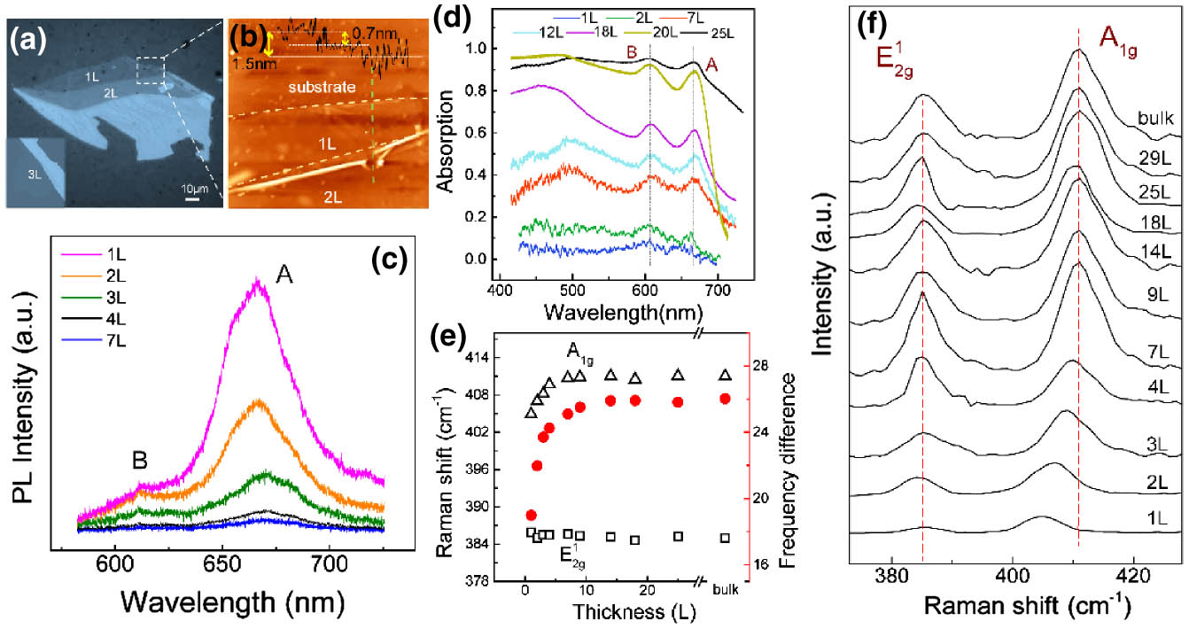
Fig. 1. (a) Microscopic images of mechanically exfoliated monolayer (1L), bilayer (2L), and trilayer (3L) of MoS2 nanosheets. (b) AFM image of the monolayer and bilayer, where the boundary is marked by yellow dashed-dotted lines. The height profiles are along the direction of the green dashed line. (c)–(f) PL, Raman, and linear absorption spectra of MoS2 nanosheets with different layers, exhibiting the layer-modulated Raman shift, PL intensity, and one-photon absorption.
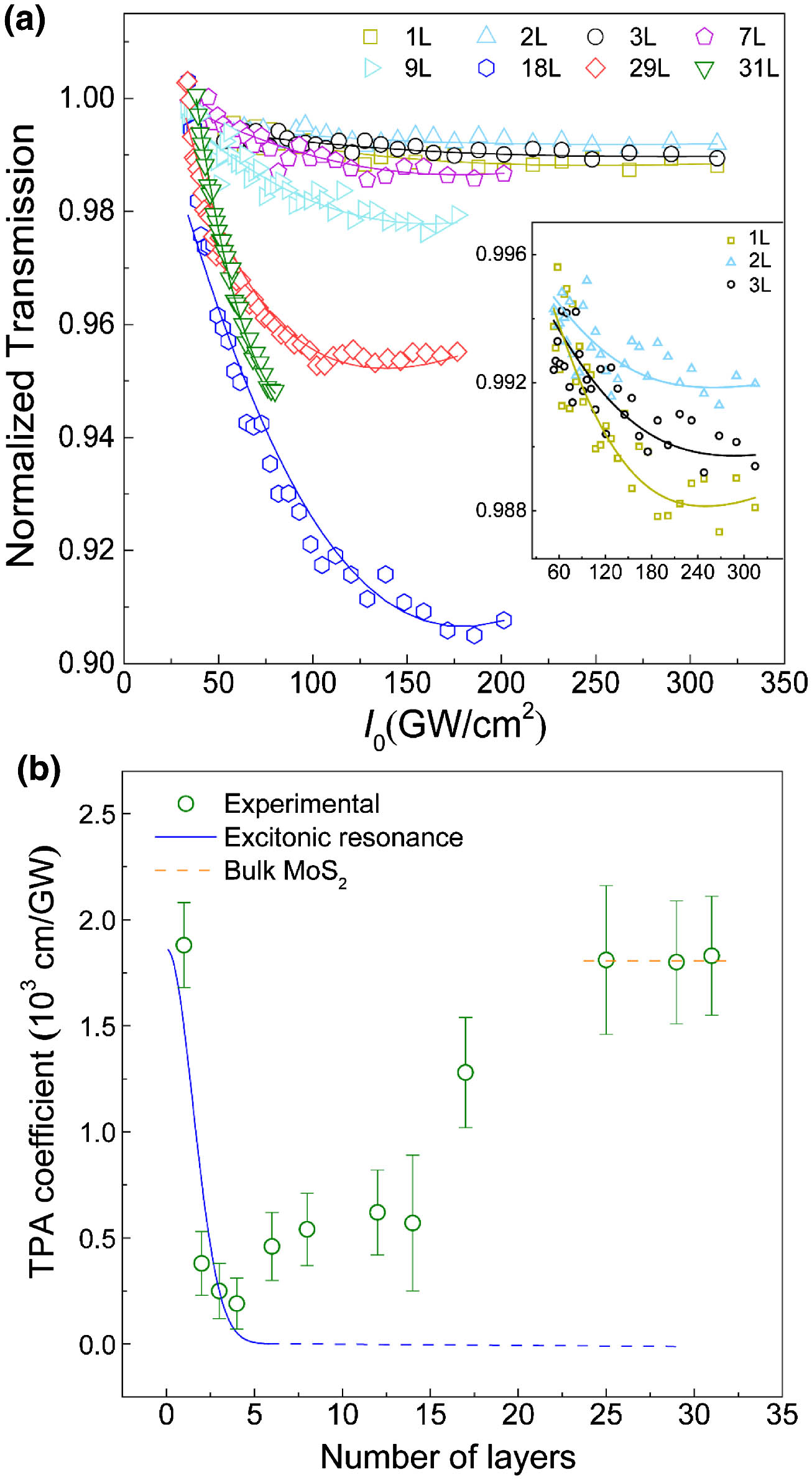
Fig. 2. (a) Micro-I-scan results for monolayer, few-layer, and multilayer MoS2, which are fitted using the homogeneously broadened TPA model. (b) TPA coefficients of layered MoS2. The green solid circle stands for the TPA coefficients, which can be separated into two parts: the trailing edge (as indicated by the blue solid line) corresponds to the excitonic resonance part, and the following rising edge corresponds to the interband transition part. The orange dashed line indicates the transition of MoS2 from the two-dimensional prototype to the bulk one.
Fig. 3. Schematic illustration of a TPA-active exciton at the K point in the Brillouin zone. 1s and 2p (∼1.88 eV and ∼2.41 eV in monolayer MoS2) represent ground state and the first excitonic dark state in a 2D non-hydrogen model. (a) In monolayer MoS2, the 2p excitonic dark state is almost in resonance with two-photon energy. (b) In few-layer MoS2, the excitonic resonance detuning increases with layer number. (c) In multilayer MoS2, the red shift of quasiparticle bandgap continues to increase, and the interband TPA occurs.
Fig. 4. Shift of the quasiparticle bandgap Eg and the first excited excitonic state (En=2) versus number of layers. As a result, the exciton binding energy (Ebn=1 and Ebn=2) decreases with layer number (bottom inset). The 1s-excitonic state locates at ∼1.88 eV [obtained from the linear absorption spectra in Fig. 1(e)] and is independent of the layer number. Here, n is the principal quantum number in the non-hydrogen model. Top inset: increase of the dielectric parameter (εn=1, εn=2) with layers. The dashed lines are intended as a visual guide.
Fig. 5. Green circles represent the TPA coefficients of ∼25LMoS2 obtained at different excitation photon energies. The peak at ∼1.21 eV is ascribed to the sub-band resonance in the conduction band. (Inset: schematic of two-photon resonant transition from valence band to a sub-band in the conduction band.) The dashed-dotted line is intended as a visual guide.
Fig. 6. Spectrum of the femtosecond laser pulse in the nonlinear optical measurements.
Fig. 7. Identification of the size of laser beam spot in our nonlinear optical measurements; the radius is ∼5 μm.
Fig. 8. AFM images of few-layer and multilayer MoS2.
Fig. 9. Complete micro-I-scan fitting results of monolayer, few-layer, and multilayer MoS2, according to the homogeneously broadened TPA model.
Fig. 10. Schematic diagram of the setup of micro-intensity scan.
Sample | Thickness (nm) | TPA Coefficient | Saturation Intensity | ME-1L | | | | ME-2L | | | | ME-3L | | | | ME-4L | | | | ME-7L | | | | ME-9L | | | | ME-12L | | | | ME-14L | | | | ME-18L | | | | ME-25L | | | | ME-29L | | | | ME-31L | | | |
|
Table 1. Complete Parameters of Thickness and NLO Coefficients
Layers | | | | | | | | 1 | 2.8a | 1.49 | 2.759a | 1.88 | 2.412 | 0.879 | 0.347 | 2 | 3.55 | 1.74 | 2.427a | 1.86 | 2.175 | 0.567 | 0.252 | 3 | 3.96 | 1.89 | | N.A. | 2.105 | N.A. | 0.214 | 4 | 3.90 | 1.86 | | N.A. | 2.113 | N.A. | 0.220 | 7 | 4.16 | 1.96 | | 1.85 | 2.079 | 0.428 | 0.199 | 9 | 4.23 | 1.98 | | N.A. | 2.069 | N.A. | 0.195 | 12 | 4.31 | 2.01 | | 1.88 | 2.062 | 0.371 | 0.189 | 14 | 4.26 | 1.99 | | N.A. | 2.066 | N.A. | 0.193 | 18 | 5.00 | 2.26 | | 1.85 | 2.005 | 0.305 | 0.150 | 25 | 5.62 | 2.49 | | 1.88 | 1.975 | 0.218 | 0.123 | 29 | 5.60 | 2.48 | | N.A. | 1.976 | N.A. | 0.124 | 31 | 5.64 | 2.50 | | N.A. | 1.974 | N.A. | 0.122 | Bulk | 5.60 | 2.48 | 2.099a | 1.88 | 1.976 | 0.219 | 0.123 |
|
Table 2. Dielectric Parameters (, ), Quasiparticle Bandgap , Energy Level, and Binding Energy for and Excitonic States from Monolayer to Multilayer