Yafeng Xie1、2, Saifeng Zhang1、6, Yuanxin Li1, Ningning Dong1, Xiaoyan Zhang1, Lei Wang1、2, Weimin Liu3, Ivan M. Kislyakov1, Jean-Michel Nunzi1、4, Hongji Qi1, Long Zhang1, and Jun Wang1、2、5、*
1Laboratory of Micro-Nano Optoelectronic Materials and Devices and CAS Key Laboratory of Materials for High-Power Laser, Shanghai Institute of Optics and Fine Mechanics, Chinese Academy of Sciences, Shanghai 201800, China
2Center of Materials Science and Optoelectronics Engineering, University of Chinese Academy of Sciences, Beijing 100049, China
3School of Physical Science and Technology, ShanghaiTech University, Shanghai 201210, China
4Department of Physics, Engineering Physics & Astronomy and Department of Chemistry, Queen’s University, Kingston, Ontario K7L-3N6, Canada
5State Key Laboratory of High Field Laser Physics, Shanghai Institute of Optics and Fine Mechanics, Chinese Academy of Sciences, Shanghai 201800, China
Yafeng Xie, Saifeng Zhang, Yuanxin Li, Ningning Dong, Xiaoyan Zhang, Lei Wang, Weimin Liu, Ivan M. Kislyakov, Jean-Michel Nunzi, Hongji Qi, Long Zhang, Jun Wang. Layer-modulated two-photon absorption in MoS2: probing the shift of the excitonic dark state and band-edge[J]. Photonics Research, 2019, 7(7): 762
Copy Citation Text
Questions hovering over the modulation of bandgap size and excitonic effect on nonlinear absorption in two-dimensional transition metal dichalcogenides (TMDCs) have restricted their application in micro/nano optical modulator, optical switching, and beam shaping devices. Here, degenerate two-photon absorption (TPA) in the near-infrared region was studied experimentally in mechanically exfoliated from single layer to multilayer. The layer-dependent TPA coefficients were significantly modulated by the detuning of the excitonic dark state (). The shift of the quasiparticle bandgap and the decreasing of exciton binding energy with layers were deduced, combined with the non-hydrogen model of excitons in TMDCs and the scaling rule of semiconductors. Our work clearly demonstrates the layer modulation of nonlinear absorption in TMDCs and provides support for layer-dependent nonlinear optical devices, such as optical limiters and optical switches.
1. INTRODUCTION
Layered transition metal dichalcogenides (TMDCs) exhibit unique nonlinear optical (NLO) properties, including high-order harmonic generation, ultrafast saturable absorption, optical limiting, multi-photon absorption, and so on [1–5]. Intrinsically, mono- and few-layered TMDCs possess large excitonic effects. Recently, the existence of excitonic dark states in monolayers (MLs) and has been revealed via two-photon photoluminescence (TPL) spectroscopy, demonstrating their potential application in optoelectronic and quantum devices [6–9]. However, it should be noted that the TPL technique is applicable only to photoluminescent materials, whereas most TMDCs, especially multilayered ones, are with low-quantum-yield or nonluminous, hampering the investigation of layer modulation (essentially excitonic dark state modulation) on the NLO absorption of TMDCs. In this work, we probed the degenerate two-photon absorption (TPA) of two-dimensional (2D) directly utilizing an NLO intensity scan setup (micro-I-scan) for micro/nano materials [10,11]. The TPA coefficients of ranging from ML to 31 layers (31L) were obtained, which were deeply modulated by the detuning of the excitonic dark state. Using a non-hydrogen model in combination with the scaling rule of semiconductors [12], the shift of the quasiparticle bandgap and the excitonic dark state with van der Waals layers were deduced [13–15]. In addition, the sub-band resonance in the conduction band was also observed in multilayer .
2. MATERIALS AND CHARACTERIZATION
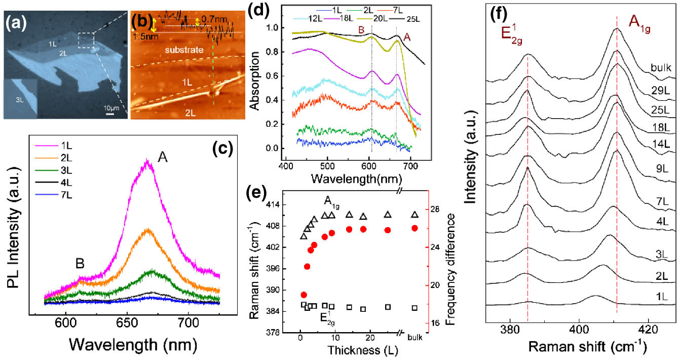
Layered nanosheets were mechanically exfoliated from the bulk crystal [16,17], and then transferred to a quartz substrate, which would affect the light absorption extremely weakly [18,19]. As shown in Fig. 1(a), the morphology of the samples can be readily identified using a objective lens. The lateral size of the samples was determined to be 10 to 100 µm, which is suitable for our NLO measurements. Raman spectroscopy and photoluminescence (PL) spectroscopy were performed, shown in Fig. 1. Both the Raman and PL signals were collected using a confocal microscopy setup (Horiba Co., HR Evolution) with a green continuous-wave (CW) laser at 532 nm ( at focus). The exact thickness of all samples was measured using atomic force microscopy (AFM). Figure 1(b) shows the thickness of the mono- and bilayer . Additional AFM images are provided in the Appendices (Fig. 8).
Figure 1.(a) Microscopic images of mechanically exfoliated monolayer (1L), bilayer (2L), and trilayer (3L) of nanosheets. (b) AFM image of the monolayer and bilayer, where the boundary is marked by yellow dashed-dotted lines. The height profiles are along the direction of the green dashed line. (c)–(f) PL, Raman, and linear absorption spectra of nanosheets with different layers, exhibiting the layer-modulated Raman shift, PL intensity, and one-photon absorption.
As shown in Fig. 1(f), two Raman-active modes, and , exhibit significant layer dependence. The Raman shifts of mono-, bi-, and trilayers are , , and , respectively, which are consistent with previous literature results [4,20]. In addition, the two Raman vibration modes provide strong evidence that all the samples used in our work are 2H-MoS2[4,21]. The PL spectra of were obtained under the same incident power. As shown in Fig. 1(c), there are two peaks at 670 nm and 615 nm corresponding to the A and B excitonic () ground states, which come from energy splitting () near the valence-band maximum due to spin-orbit coupling [22–25]. The linear absorption spectra were achieved using a confocal microscope, which are plotted in Fig. 1(e). It should be noted that there is a slight shift of the two distinct excitonic absorption peaks with layer number, but the strong excitonic effect still exists.
Sign up for Photonics Research TOC. Get the latest issue of Photonics Research delivered right to you!Sign up now
3. RESULTS AND DISCUSSION
A. Two-Photon Absorption Properties
The TPA process in layered was investigated using a micro-I scan setup [10], which integrates a microscopic imaging system (Fig. 10). The femtosecond laser pulses (pulse width: 340 fs, repetition rate: 1 kHz) at 1030 nm (1.204 eV) were generated from a mode-locked fiber laser. The laser beam was finally focused down to a spot with a waist radius of on the surface of the (Fig. 7). The intensity of the incident pulses was adjusted continuously with a linearly adjustable attenuator. The process that accounts for one- and two-photon absorption can be described by the propagation equation [2,10,11,26–29]: Here, is the propagation distance of the laser beam in the sample. is the one-photon (linear) absorption coefficient, which cannot contribute to the total absorption significantly owing to the smaller value of the photon energy of 1.2 eV than the optical bandgap [30–32]. is the TPA coefficient. In our experiment, the excitation laser source was a series of Gaussian pulses, i.e., where and represent the radius of the pump beam waist and the pulse width, respectively.
Compared with previous research on CdS nanocrystals [33], nanosheets have a uniform surface morphology with few defects in such a single crystal. Therefore, the homogeneously broadened saturation model of TPA was taken into account as follows [34,35]: where is the saturation intensity of TPA. Based on this model, the numerical fitting curves are shown in Fig. 2(a), which agree well with the experimental results (Fig. 9). The TPA coefficients of the layered were extracted, and the detailed parameters are given in Table 1 in the Appendices. As shown in Fig. 2(b), monolayer exhibits the largest TPA coefficient, which declines rapidly until approximately four layers. After that, the TPA coefficient gradually increases with layer number. This anomalous tendency reveals the switching of the optical transition from the excitonic type to the interband one, which will be discussed in the following section.
Sample
Thickness (nm)
TPA Coefficient (β0)(103cm/GW)
Saturation Intensity (Isat)(102GW/cm2)
ME-1L
∼0.7
1.88±0.21
1.98±0.16
ME-2L
∼1.4
0.38±0.15
2.05±0.24
ME-3L
∼2.1
0.25±0.13
2.59±0.13
ME-4L
∼3.0
0.19±0.12
4.08±0.28
ME-7L
∼5.0
0.46±0.16
2.52±0.24
ME-9L
∼6.3
0.54±0.17
2.19±0.21
ME-12L
∼8.4
0.62±0.20
0.97±0.15
ME-14L
∼9.8
0.57±0.32
1.27±0.16
ME-18L
∼11.9
1.28±0.26
1.82±0.17
ME-25L
∼16.8
1.81±0.35
1.18±0.18
ME-29L
∼20.3
1.80±0.39
0.42±0.12
ME-31L
∼21.7
1.83±0.28
0.70±0.15
Table 1. Complete Parameters of Thickness and NLO Coefficients
Figure 2.(a) Micro-I-scan results for monolayer, few-layer, and multilayer , which are fitted using the homogeneously broadened TPA model. (b) TPA coefficients of layered . The green solid circle stands for the TPA coefficients, which can be separated into two parts: the trailing edge (as indicated by the blue solid line) corresponds to the excitonic resonance part, and the following rising edge corresponds to the interband transition part. The orange dashed line indicates the transition of from the two-dimensional prototype to the bulk one.
Due to the 2D geometry of monolayer and poor dielectric screening, the ground-state excitons are well confined with a binding energy of [25]. This is much larger than that of traditional semiconductors and quantum wells (dozens of meV) [36,37]. As shown in Figs. 1(d) and 1(e), the PL and absorption peaks indicate that the A exciton ground state energy level () of all layered is almost the same, with a value of approximately 1.85–1.88 eV. However, the quasi-particle bandgap is much larger than the optical one according to theoretical predictions [38]. For example, is about 2.7 eV for the monolayer [25] and 2.427 eV for the bilayer [38]. Moreover, Qiu et al. have theoretically predicted that there are several excitonic dark states between 1.88 eV and 2.7 eV in monolayer . According to the transition selection rules, one-photon excitation couples states of opposite parity, as opposed to TPA, which couples states of identical parity [6]. One-photon can excite an electron only to the excitonic ground state () or any other higher-order bright excitonic states. Considering the valley polarization or different valleys in , we note that there exists the valley-selective circular dichroism arising from its unique symmetry. However, in our experiment, we used a linear polarization excitation source rather than a circular one. Both valleys ( and ) will be populated. In the meanwhile, the valley polarization is obvious only at low temperature. For example, Cao et al. measured the circularly polarized PL of monolayer () at 83 K [39], Zeng et al. gave at 10 K [40], and Mak et al. confirmed that at 14 K [41]. We did the TPA measurements at room temperature (about 300 K), at which the phonon-assisted inter-valley scattering becomes important and the valley polarization effect becomes very weak and can be neglected [42]. Hence, the TPA technique is the most effective method to study excitonic dark state transition in mono- and few-layer . In multilayer , the red shift of quasiparticle bandgap continues to increase and so do the high excited excitonic states, which leads to a large detuning between excitonic dark state and two-photon excitation [38,43]. Thus, the TPA coefficient can be modulated by the on–off resonance. In addition, it has been calculated that the transition matrix elements for direct transitions would vary with the number of layers. However, the matrix element at the point is always the strongest position [44,45].
B. Theoretical Analysis
In 2D, the hydrogen model employs an effective mass Hamiltonian , where is locally screened attractive electron–hole interaction. Depending on this model, the excitonic energy level in TMDCs can be calculated using Eq. (4) [46]: where is the binding energy of the exciton state, is the quasiparticle bandgap, is the th-order excitonic energy level, and is the excitonic principal quantum number. However, the description of 2D excitons is complicated by the fact that the screening cannot be assumed to be local. Therefore, Chernikov et al. considered a nonlocally screened electron–hole interaction described by the potential , where and are Struve and Bessel functions, and numerically calculated the radially symmetric excitonic Hamiltonian. From another point of view, the dielectric screening parameter is no longer a constant, which should be an -dependent value. The analytical expression for the nonlocal 2D screening depends on the excitonic mass and 2D polarizability [15]: Here, is the exciton reduced mass, is the 2D polarizability, the internal polarizability of the 2D dielectric [15,47], and is the -dependent effective screening dielectric parameter.
Combining Eqs. (4) and (5), we can obtain the energy levels of the A-excitonic state () of monolayer and bilayer, which are 2.412 eV and 2.175 eV, respectively. The detail of the calculation can be found in the Appendices. It is worth noting that the excitonic dark state energy level is slightly lower than that of , which is another different feature compared to the regular hydrogen model of exciton [48–50]. At a given excitonic principal quantum number , excitonic states with the higher angular momentum have a larger binding energy, which has been observed in the case of the 2H-WS2 monolayer [6,51]. Based on the theoretical estimation, the dark state of A-exciton in a monolayer (slightly lower than 2.412 eV) is almost in resonance with our two-photon energy (2.408 eV) [52]. Thus, we attribute the giant TPA coefficient in the monolayer at 1030 nm to this effect. When the number of layers is increased, the detuning between the dark state of A-exciton and the two-photon energy becomes larger, as illustrated in Fig. 3. This leads to the sharp decline of the TPA coefficient. The decline trend can be fitted using a typical TPA resonance model, in the form of where is the two-photon transition rate, is a photon energy-independent constant, and is an ideal delta function that denotes the resonance with the -excitonic state. However, the excitonic states in monolayer and few-layer are not ideally discrete. They are practically broadened with a Lorentzian profile [46,53]. The theoretical fitting of the TPA coefficient is illustrated as the blue solid line in Fig. 2(b), which is consistent with the Lorentzian function. It can be seen that the fitting curve agrees well with the experimental results from monolayer to four layers. Therefore, the sharp decline of the TPA coefficient from monolayer to few-layer can be ascribed to the detuning of excitonic dark state resonance. The contribution of excitonic dark states with larger is negligible. Such states have much smaller transition matrix elements, and they will be much harder to be populated, which means that the -excitonic state is more difficult to excite than the .
Figure 3.Schematic illustration of a TPA-active exciton at the point in the Brillouin zone. and ( and in monolayer ) represent ground state and the first excitonic dark state in a 2D non-hydrogen model. (a) In monolayer , the excitonic dark state is almost in resonance with two-photon energy. (b) In few-layer , the excitonic resonance detuning increases with layer number. (c) In multilayer , the red shift of quasiparticle bandgap continues to increase, and the interband TPA occurs.
As the thickness of is increased from a single layer to multilayers, the interaction between the van der Waals layers gets stronger, and both the quasiparticle bandgap and the binding energy of the excitons decrease [38]. Consequently, when the quasiparticle bandgap is less than 2.4 eV, TPA can occur from the valence band to conduction band. In this case, the quasiparticle bandgap can be estimated by the scaling rule applicable to most semiconductors, including multilayer TMDCs [54–57]: where is a material-independent constant, is the linear refractive index of the material, and (related to the Kane momentum parameter) is nearly material independent for a wide variety of semiconductors. By taking parabolic bands near the point in the first Brillouin zone into consideration, the function is given by [54] is about 21 eV, the same order of magnitude as previous results [54,55,58]. is about , larger than that of traditional semiconductors [56], implying strong exciton effect in TMDCs. It can be seen in Fig. 2(b) that gradually reaches a constant value when the layer number increases to about 25. It indicates that layered with such thickness has a similar TPA performance as the bulk, i.e., they are substantially bulk .
Combining Eqs. (7) and (8), the relationship between and layer number was obtained for the multilayer , as shown in Fig. 4. Then the exciton ground state and first excited state can be determined using Eq. (5). The corresponding excitonic dark state in a multilayer can be approximately marked by (i.e. ), neglecting the slight difference (smaller than 0.05 eV) [49]. The shift of the conduction band-edge (corresponding to quasiparticle bandgap ) and the dark state of A exciton (adjacent to ) is clearly demonstrated in Fig. 4. The energy distance between and becomes gradually smaller, meaning that the high excitonic states are compressed and the binding energy weakens when layer number increases. The full set of the parameters, , , , and , from monolayer to multilayer are summarized in Table 2. The increasing tendency of the dielectric parameter with layer number is obvious, which implies an increase of the dielectric screening potential. The quasiparticle bandgap and drop to almost a constant when the layer number increases to 25, which is evidence of the transition from 2D to bulk.
Layers
εn=1
εn=2
Eg(eV)
En=1(eV)
En=2(eV)
Ebn=1
Ebn=2
1
2.8a
1.49
2.759a
1.88
2.412
0.879
0.347
2
3.55
1.74
2.427a
1.86
2.175
0.567
0.252
3
3.96
1.89
2.319±0.022
N.A.
2.105
N.A.
0.214
4
3.90
1.86
2.333±0.020
N.A.
2.113
N.A.
0.220
7
4.16
1.96
2.278±0.021
1.85
2.079
0.428
0.199
9
4.23
1.98
2.264±0.022
N.A.
2.069
N.A.
0.195
12
4.31
2.01
2.251±0.025
1.88
2.062
0.371
0.189
14
4.26
1.99
2.259±0.036
N.A.
2.066
N.A.
0.193
18
5.00
2.26
2.155±0.030
1.85
2.005
0.305
0.150
25
5.62
2.49
2.098±0.042
1.88
1.975
0.218
0.123
29
5.60
2.48
2.099±0.046
N.A.
1.976
N.A.
0.124
31
5.64
2.50
2.096±0.033
N.A.
1.974
N.A.
0.122
Bulk
5.60
2.48
2.099a
1.88
1.976
0.219
0.123
Table 2. Dielectric Parameters (, ), Quasiparticle Bandgap , Energy Level, and Binding Energy for and Excitonic States from Monolayer to Multilayer
Figure 4.Shift of the quasiparticle bandgap and the first excited excitonic state () versus number of layers. As a result, the exciton binding energy ( and ) decreases with layer number (bottom inset). The -excitonic state locates at [obtained from the linear absorption spectra in Fig. 1(e)] and is independent of the layer number. Here, is the principal quantum number in the non-hydrogen model. Top inset: increase of the dielectric parameter (, ) with layers. The dashed lines are intended as a visual guide.
To further confirm the excitonic energy compression and the shift of the conduction band-edge, we investigated the excitation photon energy-dependent TPA process in , which can be treated as a bulk semiconductor. A wavelength-tunable femtosecond system (35 fs, 1 kHz, TOPAS, Coherent Co.) pumped by a Ti:sapphire laser at 800 nm was used for these measurements. As shown in Fig. 5, the TPA coefficient approximately increases with the excitation photon energy, in good agreement with the scaling rule in Eq. (7). We noticed that there is a distinct peak at about 1.21 eV. Since the quasiparticle bandgap of 25L is below 2.1 eV as given in Table 2, TPA (at photon energy ) of the electrons in the valence band can transit deep into the conduction band; this peak was ascribed to the sub-band resonance [59].
Figure 5.Green circles represent the TPA coefficients of obtained at different excitation photon energies. The peak at is ascribed to the sub-band resonance in the conduction band. (Inset: schematic of two-photon resonant transition from valence band to a sub-band in the conduction band.) The dashed-dotted line is intended as a visual guide.
In summary, we prepared monolayer, few-layer, and multilayer nanosheets through mechanical exfoliation. Using the micro-I-scan technique, we studied the TPA properties in 2D layered and found that the TPA coefficient decreased rapidly from monolayer to few-layer, and increased gradually from few-layer to multilayer up to 25 layers. Combining the non-hydrogen model of excitons in TMDCs with the scaling rule in semiconductors, we deduced the red shift of the excitonic dark state and the band-edge of conduction band with increasing layer number. The quasiparticle bandgap and excitonic dark levels, as well as the binding energy of the exciton dark state dropped dramatically until the layer number increased to 25L, which implies this is the 2D-to-bulk transition point. The sharp decline of the TPA coefficient from monolayer to 2L–4L was ascribed to the on–off resonance of excitonic dark states. In addition, the sub-band resonance in the conduction band was demonstrated. Our results provide valuable insights into the mechanism of the evolution of band structure and excitonic levels in layered , which can be applied to other TMDCs.
Acknowledgment
Acknowledgment. The authors acknowledge the utilization of equipment in the School of Physical Science and Technology in ShanghaiTech University. Y. F. Xie is grateful for the detailed discussion with Prof. Jean-Michel Nunzi.
Appendix A
In our TPA measurement, the femtosecond pulses centered at 1030 nm are generated from a mode-locked fiber laser. The pulse width is about 10 nm, i.e., the spectral width is , which is measured using the PG2000 (Ideaoptics) fiber optic spectrometer (see Fig. 6). It is much narrower than that of a Ti:sapphire femtosecond laser. Therefore, resonance excitation should occur between the conduction band maximum (CBM) and the excited excitonic state.
Figure 6.Spectrum of the femtosecond laser pulse in the nonlinear optical measurements.
In monolayer, the first-order effective screening is given by Ref. [38] in the text: Combined with Eqs. (B1) and (B2), we can get that and .
Meanwhile, we can obtain the value of of , and of , which are assumed as constants in few-layer and multilayer . Hence, we can calculate the , , and of few-layer and multilayer , as shown in Table 2.
Yafeng Xie, Saifeng Zhang, Yuanxin Li, Ningning Dong, Xiaoyan Zhang, Lei Wang, Weimin Liu, Ivan M. Kislyakov, Jean-Michel Nunzi, Hongji Qi, Long Zhang, Jun Wang. Layer-modulated two-photon absorption in MoS2: probing the shift of the excitonic dark state and band-edge[J]. Photonics Research, 2019, 7(7): 762