Zhen Yang, Yuefeng Wang, Huimin Jin, Zhiyuan Wang, Peipeng Xu, Wei Zhang, Weiwei Chen, Shixun Dai. Review of chalcogenide glass integrated photonic devices (Invited)[J]. Infrared and Laser Engineering, 2022, 51(3): 20220152
Search by keywords or author
- Infrared and Laser Engineering
- Vol. 51, Issue 3, 20220152 (2022)
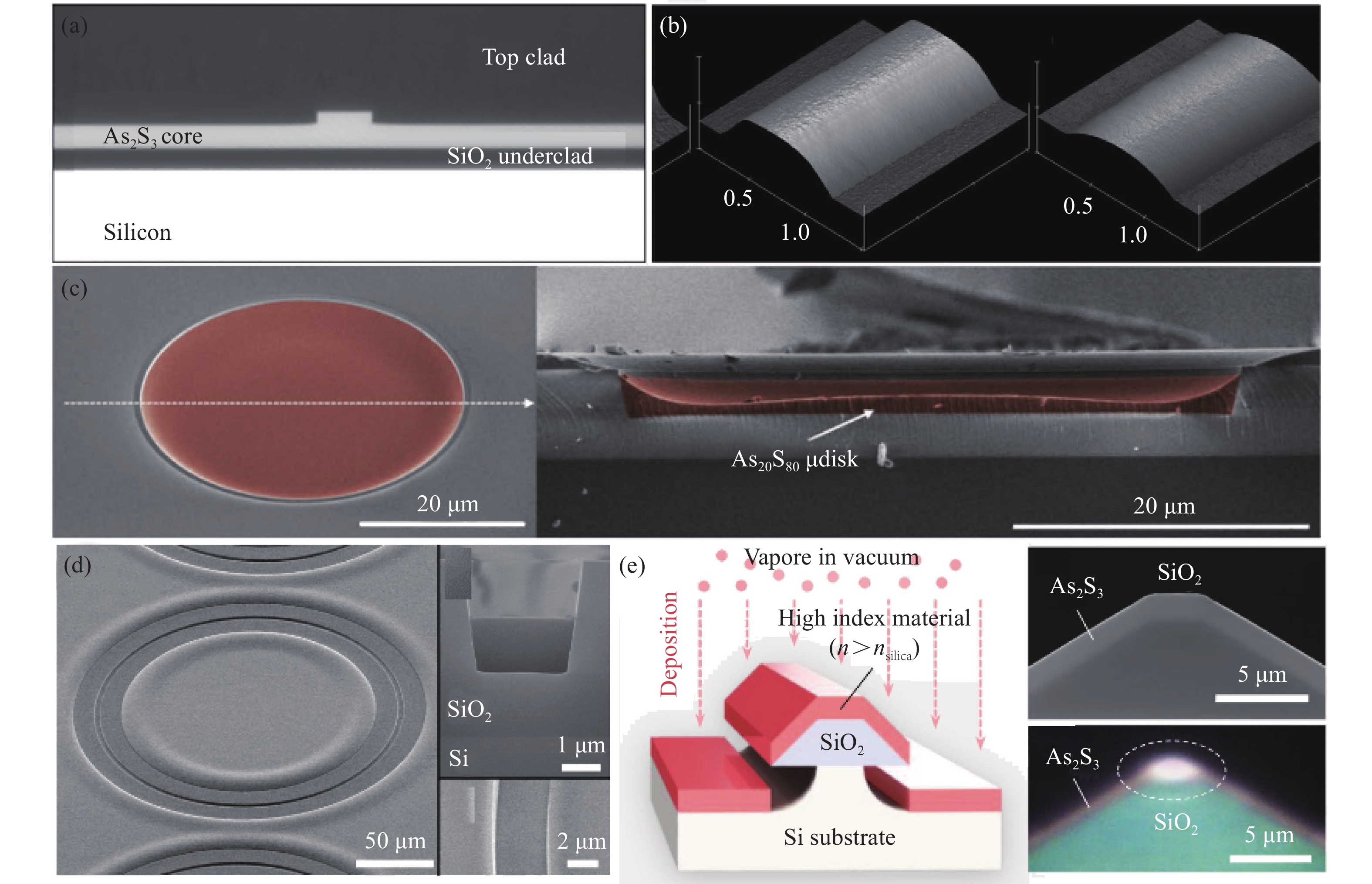
![(a) Optical micrograph of 4 µm×2.6 µm As2S3 snakes strip waveguide[24]; (b) AFM picture of As2S3 waveguide sidewall roughness after thermal annealing[25]; (c) Scanning Electron Microscopy (SEM) and cross-section of As20S80 disk resonator[26]; (d) SEM and cross-section of As20S80 microring resonator[27]; (e) Depositing the As2S3core material on the SiO2 platform structure, and SEM of cleaved cross-section of waveguide[28]](/richHtml/irla/2022/51/3/20220152/img_1.jpg)
Fig. 1. (a) Optical micrograph of 4 µm×2.6 µm As2S3 snakes strip waveguide[24]; (b) AFM picture of As2S3 waveguide sidewall roughness after thermal annealing[25]; (c) Scanning Electron Microscopy (SEM) and cross-section of As20S80 disk resonator[26]; (d) SEM and cross-section of As20S80 microring resonator[27]; (e) Depositing the As2S3core material on the SiO2 platform structure, and SEM of cleaved cross-section of waveguide[28]
![(a) SEM cross-sectional view image of GeAsSe waveguide[33]; (b) SEM image of a GeSbS microresonator[36]; (c) SEM image of a Ge28Sb12Se60 microdisk resonator[37]; (d) SEM image of a Ge28Sb12Se60 microring[38]; (e) SEM top-view image of a suspended GeAsSe microdisk resonator[33]; (f) Lorentzian fit to the resonance dip[36]; (g) Lorentzian fit to the resonance dip at 1559.657 nm[37]; (h) Lorentzian fit to the resonance dip[38]](/richHtml/irla/2022/51/3/20220152/img_2.jpg)
Fig. 2. (a) SEM cross-sectional view image of GeAsSe waveguide[33]; (b) SEM image of a GeSbS microresonator[36]; (c) SEM image of a Ge28Sb12Se60 microdisk resonator[37]; (d) SEM image of a Ge28Sb12Se60 microring[38]; (e) SEM top-view image of a suspended GeAsSe microdisk resonator[33]; (f) Lorentzian fit to the resonance dip[36]; (g) Lorentzian fit to the resonance dip at 1559.657 nm[37]; (h) Lorentzian fit to the resonance dip[38]
Fig. 3. (a) 200 μm radius microdisk resonator; (b) Simulated field intensity profile of the fundamental mode of the microdisk resonator[22]; (c) SEM image of the cross-section of waveguide[48]
Fig. 4. (a) Schematic diagram and SEM image of the Ge23Sb7S70 spiral waveguide[54]; (b) Cross-sectional view and the corresponding SEM image of the ridge waveguide comprising two different compositions of GeSeSe glasses[61]; (c) Schematic diagram and cross-sectional SEM image of the the ZnSe rib waveguide[63]; (d) Cross-sectional SEM image of the Ge28Sb12Se60 strip waveguide and schematic diagram of the waveguide integrated with a PDMS gas cell[56]; (e) Schematic diagram of the Ge28Sb12Se60 waveguide sensor using the silver island film[64]
Fig. 5. (a) Schematic, electric field distribution and band diagram of the Ge11.5As24Se64.5 grating resonance sensor [68]; (b) SEM images of the Ge28Sb12Se60 waveguide sensor using micro-ring resonance [70]; (c) SEM images of the Ge28Sb12Se60 slot waveguide and the Ge28Sb12Se60 slot micro-ring sensor [71]
Fig. 6. (a) Schematic diagram of on-chip SC integrated with optical sensor [39]; (b) Schematic diagram and cross-sectional view of the optical sensor using spiral waveguide integrated with PbTe photodetector [55]
Fig. 7. (a) Typical waveguide cross section under SEM inspection[29]; (b) The simulation of supercontinuum spectrum broadening[29]; (c) Experimental results of supercontinuum spectrum generation in TM mode[29]; (d) Typical waveguide cross section under SEM inspection[52]; (e) Experimental SC evolution with increasing powers at a pump wavelength of 4.184 μm[52]
Fig. 8. (a) Overview of SBS: A pump wave (ω 1) scatters from and re-enforces an acoustic phonon (Ω ) and is downshifted to a Stokes wave (ω 2), the result is a narrow Stokes peak separated at a distance of GHz from the pump, this configuration shows backward Brillouin scattering[86]; (b) Schematic of a BL based on photonic chip[82]; (c) Schematic of the hybrid As2S3ring resonator structure, concept figure for the lasing conditions[84]; (d) SBS-based integrated microwave photonic filter, stopband center frequency tuning[83]
Fig. 9. (a) Lorentzian fit to the resonance dip of As2S3 microsphere[91]; (b) Raman emission power versus coupled pump power[91]; (c) Image of a typical packaged As2S3 microsphere[92]; (d) Lorentzian fit to the resonance dip of typical packaged As2S3 microsphere[92]; (e) Spectrum of a 5 Raman orders cascaded SRS emission of an As2S3 microsphere[92]; (f) Experimental spectrum of four-cascade Raman lasing[85]; (g) Measured Raman spectrum when increasing the pump power to ~30 mW[36]
Fig. 10. Integrated photonic chalcogenide phase-change switching. (a) Schematic of the integrated photonic SiN-on insulator platform for broadband switching operation[102]; (b) Spectral shift and loss characterization of GST using silicon microring resonators[103]; (c) Low-loss broadband directional coupler switches based on GST[104]
Fig. 11. (a) Schematic of all-optical multi-level memory based on Si3N4 microring resonator[106]; (b) Operation principle of an all-optical fully integrated on-chip multilevel memory; (c) A multibit and multiwavelength architecture[96]
Fig. 12. PCM based optical VMM and neural networks: (a) A chip-scale all-optical abacus based on GST on Si3N4[108]; (b) Photonic in-memory computing demonstrating optical scalar-scalar multiplication and matrix-vector multiplication[110]; (c) An integrated photonic tensor core enabled by an optical frequency comb and in-memory computing cell arrays[111]
|
Table 1. Current several typical chalcogenide waveguides at 1.55 µm
|
Table 2. Recent research progress of chalcogenide optical waveguide performance in mid-infrared band
|
Table 3. Research progress of on-chip mid-infrared SC output in chalcogenide waveguides

Set citation alerts for the article
Please enter your email address


