Chang-Lin WU, Chang WANG, Jun-Cheng CAO. Numerical simulation of scanning nearfield optical microscopy based on the source dipole model[J]. Journal of Infrared and Millimeter Waves, 2023, 42(5): 643
Search by keywords or author
- Journal of Infrared and Millimeter Waves
- Vol. 42, Issue 5, 643 (2023)
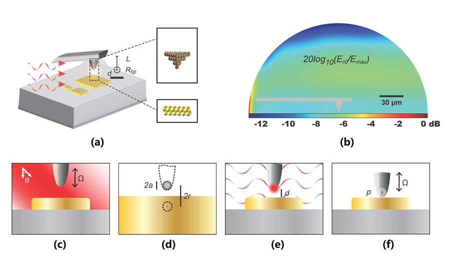
![Physical and mathematical modeling of s-SNOM. (a) The AFM probe works in tapping mode, with the tip-sample junction distance varying, causing strong interatomic and near-field interactions. Tip length L, radius Rtip and distance d is shown in (a). (b) Field distribution calculated on the sphere surface 20lg[E(r=r0)/max(E)]. Here, the maximum electric field strength is derived from the whole body simulation, (c) Full simulation model with a nonzero incident angle θ and tip tapping frequency Ω. (d) The PDM method considers the scattering tip as a polarized sphere with radius a, and the distance from the sphere center to the image sphere center is 2r. The FDM method can be considered as replacing the sphere in the PDM method with an ellipsoid, which takes into account the effect of part of the probe shaft. (e) Use of a z-polarized background field to excite tip enhancement at the tip apex. The boundary conditions are fixed, while the tip-sample distance d is variable. (f) Dipole source model with a realistic tip shape and a fixed dipole moment; the nonlinear phenomena caused by the tip movement in tapping can be revealed in numerical computation.](/richHtml/hwyhmb/2023/42/5/643/img_06.jpg)
Fig. 1. Physical and mathematical modeling of s-SNOM. (a) The AFM probe works in tapping mode, with the tip-sample junction distance varying, causing strong interatomic and near-field interactions. Tip length L, radius Rtip and distance d is shown in (a). (b) Field distribution calculated on the sphere surface 20lg[E(r=r0)/max(E)]. Here, the maximum electric field strength is derived from the whole body simulation, (c) Full simulation model with a nonzero incident angle θ and tip tapping frequency Ω. (d) The PDM method considers the scattering tip as a polarized sphere with radius a, and the distance from the sphere center to the image sphere center is 2r. The FDM method can be considered as replacing the sphere in the PDM method with an ellipsoid, which takes into account the effect of part of the probe shaft. (e) Use of a z-polarized background field to excite tip enhancement at the tip apex. The boundary conditions are fixed, while the tip-sample distance d is variable. (f) Dipole source model with a realistic tip shape and a fixed dipole moment; the nonlinear phenomena caused by the tip movement in tapping can be revealed in numerical computation.

Fig. 2. Analysis of the effect of the probe shaft and tip apex on SNOM imaging,simulated with the FWS method and SDM in a 30 THz EM field.(a)Schematic diagram of the SPM probe and sample interaction. Tip length L,radius Rtip and distance d. The excitation of this antenna-like probe by the electric field E generates charge oscillations and,together with the conducting sample,forms a monopole antenna that radiates signals to the far field(top right). The capacitor equivalent to the probe tip and the sample is depicted,which generates a tunneling current due to the quantum tunneling effect. The energy state of molecules can be changed when they are filled in the gap(bottom left). For a mathematical description of the probe,the probe is divided into three regions,and a circular region is defined outside the probe(bottom right).(b)Normalized Enear evaluated 1 nm directly underneath the tip apex and Efar evaluated 2λ from the tip apex for different tip lengths L.(c)Normalized Enear evaluated 1 nm directly underneath the tip apex and Efar evaluated 2λ from the tip apex for different tip apex radii Rtip. Here the normE is the absolute value of the electric field strength.
Fig. 3. Simulation application to a gold thin film. The FWS method is used to calculate the near-field enhancement with background electric field strength Ez = 3 500 V/m.(a)Spatial field distribution 20lg[E(r)/E(d = 2 nm)]calculated for gold films of different thicknesses at different tip-sample distances d using the electric field strength 1 nm below the tip apex. The field strength at d = 2 nm is set as 0 dB,(b)Change in the normalized near-field strength 1 nm under the tip apex with increasing tip-sample distance d,as depicted in(a).(c)Whole space field distribution 20lg[E(r)/E(d = 2 nm)]caused by the dipole source,calculated using the SDM method. The electric field strength is calculated 1 nm below the tip apex,and the field strength at d = 2 nm is set as 0 dB.(d)Change in the normalized far-field strength 1 nm under the tip apex of(c)with increasing tip-sample distance d,(e)Average far-field strength for various tapping amplitudes A;the data in(d)can be regarded as corresponding to A = 0 nm
Fig. 4. Simulation of the difference between near-field and far-field signals for Au samples of different sizes,grounded or not(connected to a larger metal is considered grounded).(a)The electric field distribution around the 50 nm thick gold samples is calculated at d = 50 nm. Let the electric field strength at 2 nm from apex for the 1 nm wide sample be 0 dB.(b)3D distribution of electric field strength for an isolated Au sample,(c)Simulated imaging of a sample with grounded and ungrounded gold square patches(narrowest line width of 10 nm),with a step size of 50 nm in(X,Y)scanning. Top view of the sample(top right;for details,see the Supporting Information). Grayscale plot of the near-field Ez signal(bottom left,1 000 nm × 1 000 nm). The top left and bottom right are the electric field strength distributions corresponding to the two profile lines with 256 as the maximum value,respectively

Set citation alerts for the article
Please enter your email address


