1State Key Laboratory of Electronic Thin Films and Integrated Devices, School of Optoelectronic Science and Engineering, University of Electronic Science and Technology of China, Chengdu 610054, China
2Chongqing United Microelectronics Center, Chongqing 401332, China
This paper proposes a 3- mid-infrared band polarization-independent and CMOS-compatible graphene modulator, which mainly includes two parts: the mode conversion structure and the graphene modulator. This modulator not only fulfills the requirement of compatibility with CMOS, but also can achieve polarization-independent modulation of the fundamental mode. Simulation results show that this modulator can achieve an extinction ratio(ER) higher than 20 dB in the mid-infrared band from 2.95 to 3.05 , the insert loss for both TE and TM modes are less than 1.3 dB, and polarization-dependent loss is less than 1.09 dB. Through the calculation, the 3 dB bandwidth up to 9.47 GHz can be obtained when the length of the device is 420 .
A variety of functional electro-optic materials, such as graphene[1], chalcogenide[2], and black phosphorus[3], have been discovered in recent years, which indirectly promoted the realization of high-performance electro-optic devices. Among these materials, graphene has been widely used in many fields with its unique physics properties[4-8], especially in electro-optic modulators. Compared with other materials, the advantage of graphene includes constant absorption over a wide spectrum[9], ultra-high carrier mobility under room temperature[10], controllable conductivity, and compatibility with CMOS. The light in the mid-infrared band has attracted wide attention in the fields of communications, homeland security, and biomedicine. Some electro-optic modulators operating in the mid-infrared band have been reported, but most of them are polarization-dependent[11-14], which means that the device can operate under only one polarization state.
Research work has proven that the graphene is an anisotropic material[15-16] whose lattice is only periodically arranged along the 2D surface of graphene. Graphene mainly interacts with the tangential electric field of electromagnetic waves[12], and this characteristic will lead to the interaction between the graphene horizontally embedded in the waveguide and the TM mode is much stronger, which has been confirmed in previous work[17]. In the previously reported graphene-based polarization-independent modulators[18-21], most of them need to face the problem of the complicated structure of the device, cumbersome manufacturing processes, and incompatibility with CMOS. Therefore, achieving the polarization-independent operation of the electro-optic modulator remains a challenge.
In this paper, we propose a 3- mid-infrared polarization-independent and CMOS-compatible graphene modulator. The TE0 mode of incident light is converted to the TM0 mode through a mode conversion structure, and the TM0 mode of incident light is not affected by this structure because of the phase mismatching, so we can achieve the modulation of only TM0 mode through the graphene modulator. In the structure of the graphene modulator, the graphene sheet is integrated on the chalcogenide glass to fulfill the compatibility with CMOS. Simulation results show that this modulator can achieve the polarization-independent operation in the mid-infrared band. The length of the device is designed to be 420 , we can obtain the ER higher than 20 dB, and the insert loss less than 1.3 dB. The polarization-dependent loss is maintained at a value less than 1.09 dB in the wavelength range from 2.95 to 3.05, and the 3 dB bandwidth of the device is 9.47 GHz through the calculation.
1 Principle and structure design
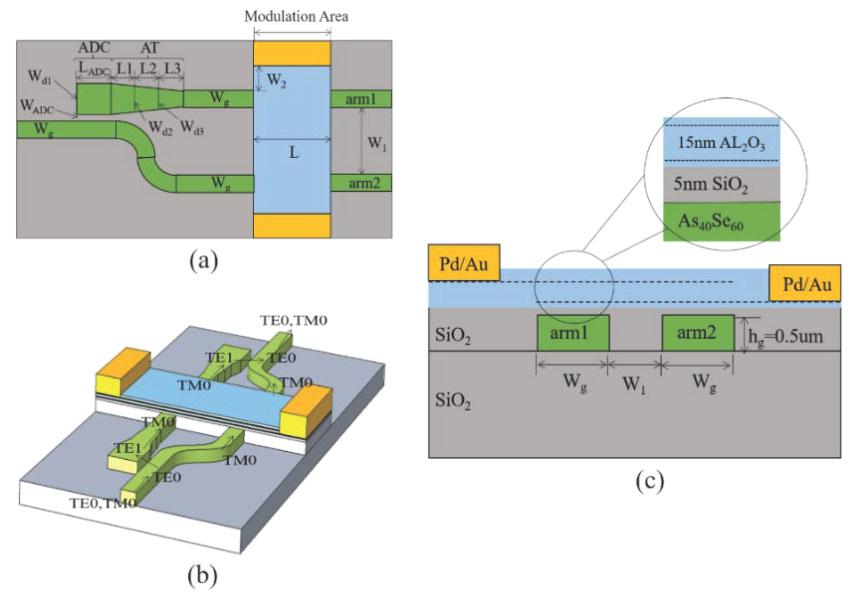
The structure of our proposed device is shown in Fig. 1(a). The device mainly includes two parts, the mode conversion structure and the graphene modulator. Since the graphene horizontally integrated on the chalcogenide glass mainly interacts with TM0 mode, we designed a mode conversion structure composed of the asymmetric directional coupler(ADC) and adiabatic taper(AT). As shown in Fig. 1(b), we designed two modulation waveguide arms in the device, the width of arm2 is 1.5 , and compared with arm 2, arm 1 adds a wide waveguide with the size of 3.1 and a tapered waveguide, the spacing between the two arms is set to 1 to prevent mode coupling. The TE0 mode is converted to TE1 mode by the ADC composed of a narrower waveguide and a wider waveguide, then the TE1 mode is converted to the TM0 mode by the AT, so we can realize the modulation of TM0 mode in the modulation area. At the output of arm1, the TM0 mode will be restored to the TE0 mode by the same mode conversion structure. In the meanwhile, the TM0 mode will not be affected when passing through the region of ADC because of phase mismatching. By using this principle, the device we proposed can achieve the same modulation capability for both TE and TM mode.
Figure 1.(a) Schematic diagram of our proposed device,(b) schematic diagram of mode conversion structure,(c) cross-sectional schematic diagram of the graphene modulator
In order to achieve polarization-independent modulation, we horizontally integrated the graphene sheet on the chalcogenide glass. When a certain voltage is applied to graphene, its chemical potential will be dynamically changed. Graphene is an anisotropic material, its vertical dielectric constant is not affected by the applied voltage and is always maintained at a value of 2.5, while the in-plane dielectric constant is determined by[10]
.
It can be seen from the formula that the in-plane dielectric constant mainly depends on the frequency of incident light and applied voltage. As shown in Fig. 2(a), under the wavelength of 2.95 , 3 , 3.05 , the variation of the in-plane dielectric constant under different graphene chemical potential is analyzed. The absorption characteristic of graphene mainly depends on its dielectric constant, Fig. 2(b) shows the variation of the absorption coefficient for both TE0 and TM0 mode under different graphene chemical potential. It can be seen that the absorption coefficient for both TE0 and TM0 modes decrease rapidly when the graphene chemical potential increases. In addition, the absorption coefficient for the TM0 mode is greater than the TE0 mode, which means that the graphene sheet has a stronger interaction with TM0 mode.
Figure 2.(a) Under the wavelength of 2.95 , 3 , 3.05 , the in-plane dielectric constant changes with the applied voltage,(b) the variation of the absorption coefficient for both TE0 and TM0 mode of graphene modulator under different chemical potential
The cross-section of the graphene modulator is shown in Fig. 1(c). By using an electron beam exposure method[22], a 0.5- thick chalcogenide glass waveguide is integrated on the silicon-based platform, then a 5 nm thick SiO2 isolation layer is thermally grown on the surface of the waveguide. Afterward, two-layer CVD-grown graphene sheets were transferred on top of the chalcogenide glass waveguide[23]. By using the thermal atom deposition method[24], two-layer graphene sheets were separated with a 15 nm thick Al2O3 to form a capacitor structure. In the meanwhile, in order to prevent the latent carrier injection, the upper and lower layer of graphene sheets were separated from the chalcogenide waveguide and the air with a 5nm thick Al2O3 isolation layer. Finally, the metal electrode Au/Pd is transferred onto the graphene sheet, in order to avoid interference with the optical mode in the waveguide, the electrode is located 0.6 away from the waveguide.
The performance of the device is simulated by using Lumerical software. The variation of the effective mode index under different width of waveguide is analyzed, as shown in Fig. 3(a), the waveguide structure is composed of SiO2 as the lower cladding, air as the upper cladding, and chalcogenide glass as the core. We analyzed the effective refractive index of the first five modes in the width range from 1.4 to 3.4 . It can be seen that the effective refractive index of TE0 mode in a width of 1.5 is close to the value of TE1 mode in a width of 3.1 , so we choose an ADC composed of these two sizes of the waveguide to achieve the conversion from TE0 to TE1 mode, and the coupling spacing is set at 0.1 . As shown in Figure 3(b), when the coupling length is 50 , the coupling efficiency up to 0.97 can be obtained, and the electric field distribution of mode coupling is shown in the inset of Figure 3(b). In addition, when the width of the waveguide is around 1.75 , the TE1 and the TM0 mode are both in the mode mixing region, so we can design a tapered waveguide with the size around 1.75 to realize the conversion from TE1 mode to TM0 mode. The width of input and output of taper is 3.1 and 1.5 , in order to achieve mode conversion, we divided the taper into three parts, the width of the input and output of the second part is set at 1.81 and 1.67 . As shown in Fig. 3(c), the influence of the length for three parts on conversion efficiency is analyzed by the simulation, the main impact on conversion efficiency are the second part, so we choose L1 = L2 = L3 = 20 to maximize the conversion efficiency and reduce the size of the device as much as possible. The electric field distribution of mode conversion is shown in the inset of Fig. 3(c).
Figure 3.(a) The variation of effective refractive index for the first five modes in the width range from 1.4 to 3.4 ,(b) analyzing the influence on coupling efficiency by sweeping the coupling length,(c) analyzing the influence on conversion efficiency by sweeping the length of three parts
We analyzed the insert loss of the device, including the mode coupling loss of the ADC(CL1), the mode conversion loss of the AT(CL2), the insert loss between the waveguide arm and the graphene modulator(IL), and the graphene absorption loss(GL). Figure 2(b) shows the variation of the absorption coefficient of the fundamental mode under different graphene chemical potential, it can be seen that when the applied voltage is 0.1 eV and 0.7 eV, the absorption coefficient reaches a maximum and minimum respectively. Therefore, we choose 0.1 eV and 0.7 eV as the “OFF” state point and the “ON” state point respectively. In order to obtain a higher ER, the length of the graphene modulator is set to 300 . As shown in Fig. 4(a), the variation on insert loss for different parts is analyzed under the wavelength range from 2.95 to 3.05 . The normalized transmission and extinction ratio of our proposed device are also analyzed, as shown in Fig. 4(b). The propagation loss under the "ON" state point is mainly determined by the absorption loss of graphene and its value is less than 1.3 dB, while under the "OFF" state point, the normalized transmission is less than -20 dB and the extinction ratio is higher than 20 dB. In order to measure the polarization-dependent loss, we analyzed the normalized transmission difference between the two modes, the results show that the polarization-dependent loss of the device is less than 1.09 dB in the wavelength range from 2.95 to 3 , which fulfills the requirement of polarization-independent modulation.
Figure 4.(a) The variation of insertion loss of various parts for the device under the wavelength from 2.95 to 3.05 ,(b) the normalized transmission of the device under the wavelength from 2.95 to 3.05
The 3 dB modulation bandwidth is also a crucial parameter for the modulator. Due to the ultrahigh carrier mobility of graphene under room temperature, the operating speed of the modulator is no longer limited by the lifetime of minority carriers. The main factor affecting 3 dB modulation bandwidth of modulator based on graphene is RC delay. The result is expressed as
,
R is the entire resistance of the device, mainly including two parts, the contact resistance between graphene sheets and electrodes, and the graphene sheets resistance , which can be calculated by
,
where is the effective width of graphene, is the spacing between two modulation arms, is the width of graphene from metal contact to the active region of the waveguide, is the length of graphene, [25] and [26] can be obtained from previous work.
C is the capacitance of the capacitor composed of two graphene sheets. To estimate the 3 dB bandwidth, we regarded the capacitor structure of the device as a parallel plate capacitor. The estimated 3 dB bandwidth is 9.47 GHz, in addition, the RC delay problem may be solved in the future, which means that a higher 3dB bandwidth can be obtained[27-28].
3 Conclusion
This paper proposes a 3- mid-infrared polarization-independent and CMOS-compatible graphene modulator. In the structure of this device, in order to achieve polarization-independent modulation, we introduce an asymmetric directional coupler and adiabatic taper structure to achieve mode conversion, and the graphene sheet is integrated on the chalcogenide glass waveguide. The simulation results show that our device can achieve an extinction ratio higher than 20 dB under the mid-infrared band from 2.95 to 3.05 , the insert loss for both two modes is less than 1.3 dB, and the polarization-dependent loss is less than 1.09 dB. These data indicate that our device fully fulfills the requirement of the polarization-independent operation. Through the calculation, when the length of the device is 420 , the 3 dB bandwidth up to 9.47 GHz can be obtained, and after solving the RC delay problem in the future, it is expected to achieve a higher 3 dB bandwidth. In short, this new type of 3 mid-infrared polarization-independent and CMOS-compatible modulator is expected to promote the development of on-chip optical communications in the future.