
Dun Pi, Zihao Shan, Xingkun Wu. Nanostructured Antireflection Micro-Optics in the Optical Fiber Communication Band[J]. Acta Optica Sinica, 2020, 40(6): 0622002
- Acta Optica Sinica
- Vol. 40, Issue 6, 0622002 (2020)
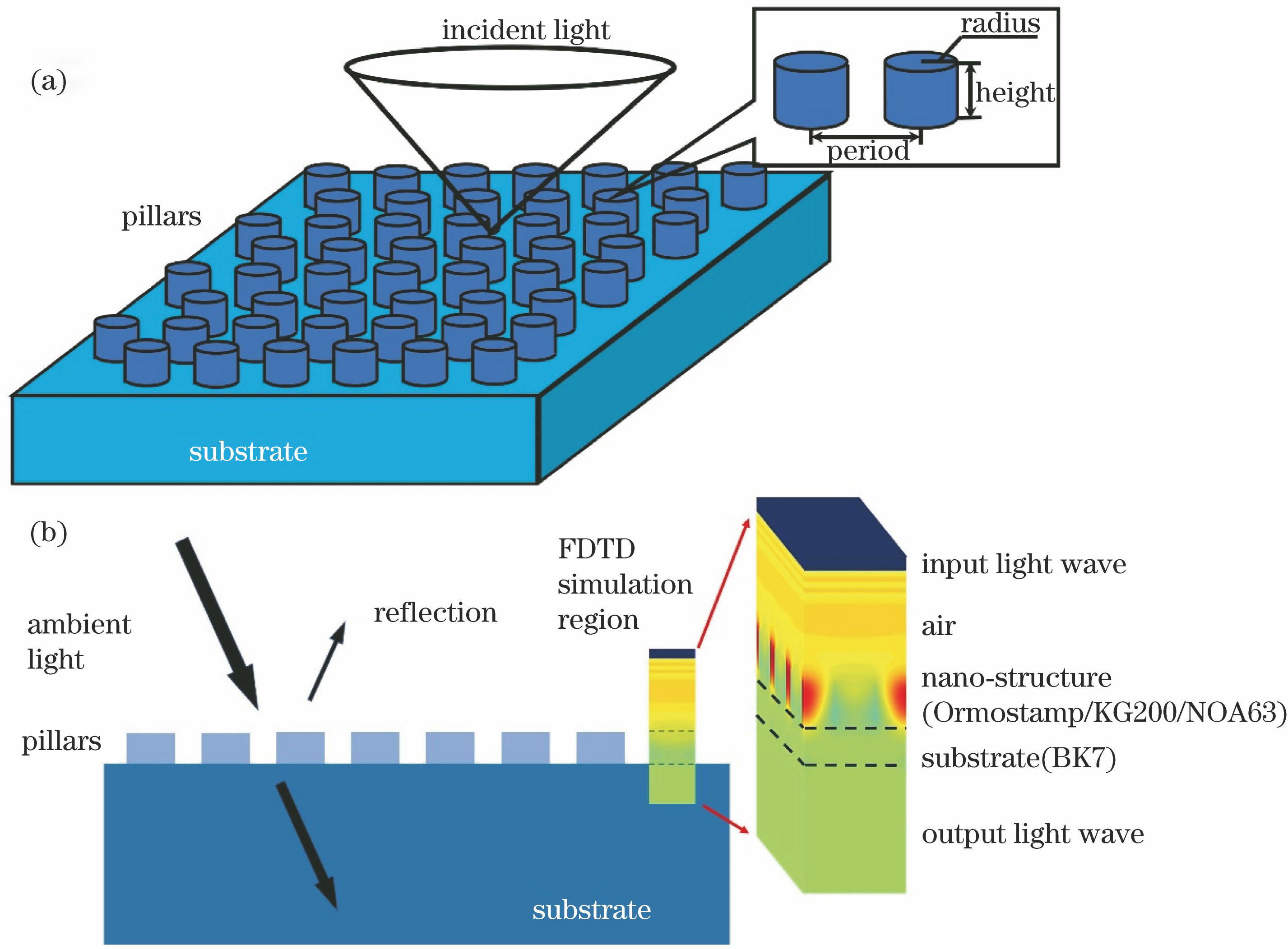
Fig. 1. Schematic of antireflection layer. (a) Distribution of the nanopillars of antireflection layer; (b) antireflection layer in FDTD simulation (material of nano-structure is UV curable optical resin, material of substrate is optical glass)
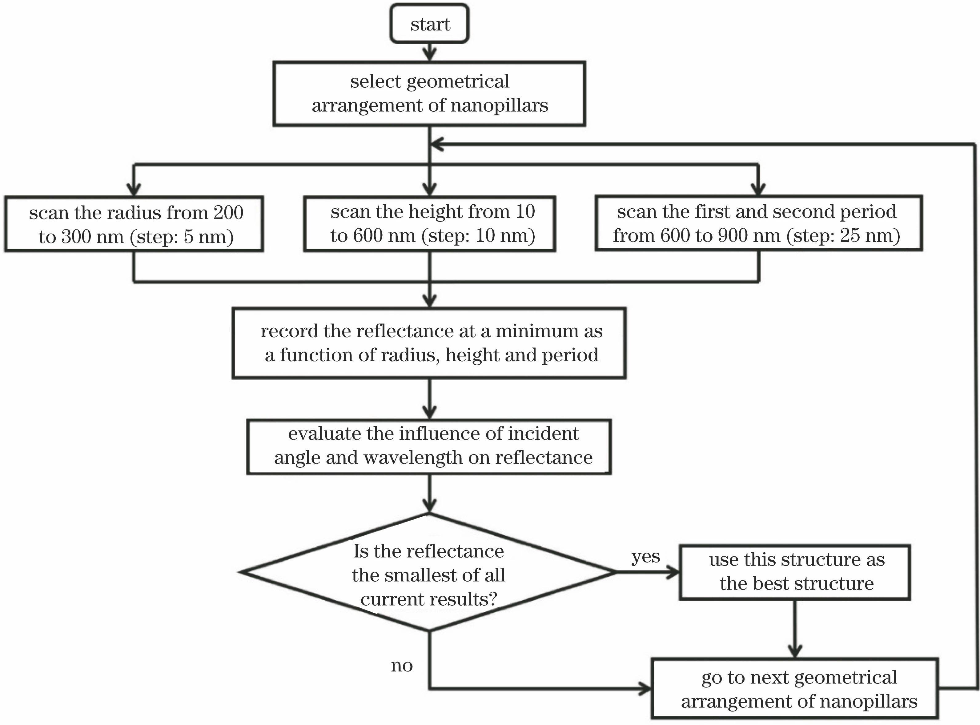
Fig. 2. Flowchart of optimization algorithm for nanopillar antireflection structure
Fig. 3. Simulation experiment results of FDTD method. (a)-(c) Numerical simulation of reflectance as a function of pillar radius, height, and period at the wavelength of 1550 nm; (d) angular dependence of reflectance on both polar and azimuth incident angles at the wavelength of 1550 nm
Fig. 4. Comparison of optimal parameter structure and other parameter structures. (a) Without antireflection structure; (b) optimal antireflection structure; (c) diameter of nanopillars deviates from optimal conditions(the diameter is 150 nm); (d) height of nanopillars deviates from optimal conditions (the height is 450 nm)
Fig. 5. Fabrication process flowchart of nanopillar structure on glass substrate for antireflection
Fig. 6. SEM images. (a) Top-view of nanopillars; (b) 45°-view of nanopillars imprinted on the glass substrate; (c)(d) top-view and side-view of nano-hole structure on PET stamp for nano-imprinting
Fig. 7. Nano antireflection structure directly imprinted on top surface of an FC/PC plug
Fig. 8. Comparison of measured reflectance with that calculated by FDTD method. The samples were imprinted with three different UV-curable polymers: Ormostamp@ (polymer 1), secondary fiber coating (polymer 2) and NOA63 (polymer 3)
Fig. 9. Measurement of water contact angle. (a) Contact angle without moth-eye nanostructure is 85.9°; (b) contact angle with moth-eye nanostructure is 111.0°

Set citation alerts for the article
Please enter your email address
© Copyright 2018-2021 | Chinese Laser Press. All Rights Reserved 沪ICP备15018463号-20