• Journal of Semiconductors
  • Vol. 43, Issue 11, 112301 (2022)
Kaixuan Chen1、2, Gengxin Chen3, Ziliang Ruan3, Xuancong Fan1、2, Junwei Zhang4, Ranfeng Gan1, Jie Liu4, Daoxin Dai3、5, Changjian Guo1、2, and Liu Liu3、5、*
Author Affiliations
  • 1Guangdong Provincial Key Laboratory of Optical Information Materials and Technology, South China Academy of Advanced Optoelectronics, South China Normal University, Higher-Education Mega-Center, Guangzhou 510006, China
  • 2National Center for International Research on Green Optoelectronics, South China Normal University, Guangzhou 510006, China
  • 3State Key Laboratory for Modern Optical Instrumentation, College of Optical Science and Engineering, International Research Center for Advanced Photonics, Zhejiang University, Hangzhou 310058, China
  • 4State Key Laboratory of Optoelectronic Materials and Technologies, School of Electronics and Information Technology, Sun Yat-Sen University, Guangzhou 510006, China
  • 5Jiaxing Key Laboratory of Photonic Sensing & Intelligent Imaging, Intelligent Optics & Photonics Research Center, Jiaxing Research Institute, Zhejiang University, Jiaxing 314000, China
  • show less
    DOI: 10.1088/1674-4926/43/11/112301 Cite this Article
    Kaixuan Chen, Gengxin Chen, Ziliang Ruan, Xuancong Fan, Junwei Zhang, Ranfeng Gan, Jie Liu, Daoxin Dai, Changjian Guo, Liu Liu. Four-channel CWDM transmitter chip based on thin-film lithium niobate platform[J]. Journal of Semiconductors, 2022, 43(11): 112301 Copy Citation Text show less
    (Color online) (Color online) Proposed four-channel CWDM transmitter on the TFLN platform. 3D view of (a) whole structure and (b) CWDM device based on the AMMI structure. (c) Cross-sectional view of the modulation section. (d) Top view of the CLTW electrode.
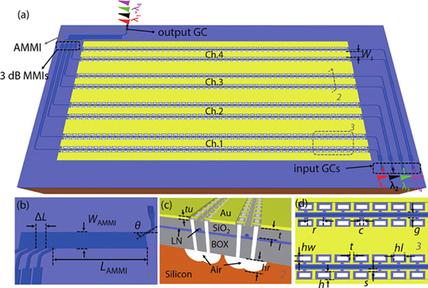
    Fig. 1. (Color online) (Color online) Proposed four-channel CWDM transmitter on the TFLN platform. 3D view of (a) whole structure and (b) CWDM device based on the AMMI structure. (c) Cross-sectional view of the modulation section. (d) Top view of the CLTW electrode.
    Optical images of (a) whole transmitter and (b) four-channel CWDM device. Scanning electron microscope images of (c) cross-sectional view and (d) top view of the modulation section.
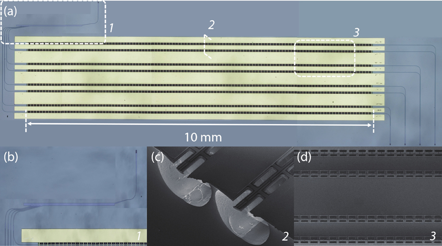
    Fig. 2. Optical images of (a) whole transmitter and (b) four-channel CWDM device. Scanning electron microscope images of (c) cross-sectional view and (d) top view of the modulation section.
    (Color online) (a) Measured and simulated transmission spectral responses of the fabricated CWDM device. (b) Measured transmission spectral responses of the four input GCs and the common output GC.
    Fig. 3. (Color online) (a) Measured and simulated transmission spectral responses of the fabricated CWDM device. (b) Measured transmission spectral responses of the four input GCs and the common output GC.
    (Color online) Normalized optical transmission of the fabricated four modulators as a function of the applied voltage for (a) Ch. 1 and Ch. 2, and (b) Ch. 3 and Ch. 4.
    Fig. 4. (Color online) Normalized optical transmission of the fabricated four modulators as a function of the applied voltage for (a) Ch. 1 and Ch. 2, and (b) Ch. 3 and Ch. 4.
    (Color online) Measured EE (a) transmissionsS12 and (b) reflectionsS11 for the four modulators.
    Fig. 5. (Color online) Measured EE (a) transmissionsS12 and (b) reflectionsS11 for the four modulators.
    (Color online) Measured EE crosstalk characteristics of the fabricated CWDM transmitter for (a) Ch. 1, (b) Ch. 2, (c) Ch. 3, and (d) Ch. 4.
    Fig. 6. (Color online) Measured EE crosstalk characteristics of the fabricated CWDM transmitter for (a) Ch. 1, (b) Ch. 2, (c) Ch. 3, and (d) Ch. 4.
    (Color online) Measured and simulated EO responses for the four modulators.
    Fig. 7. (Color online) Measured and simulated EO responses for the four modulators.
    (Color online) (a) Experimental setup for high-speed data transmission measurements. PC: polarization controller. Measured optical eye diagrams for the OOK format at a data rate of 64 Gb/s for (b) Ch. 1, (c) Ch. 2, (d) Ch. 3, and (e) Ch. 4.
    Fig. 8. (Color online) (a) Experimental setup for high-speed data transmission measurements. PC: polarization controller. Measured optical eye diagrams for the OOK format at a data rate of 64 Gb/s for (b) Ch. 1, (c) Ch. 2, (d) Ch. 3, and (e) Ch. 4.
    (Color online) Measured optical eye diagrams for the PAM-4 format at a data rate of 100 Gb/s for (a) Ch. 1, (b) Ch. 2, (c) Ch. 3, and (d) Ch. 4.
    Fig. 9. (Color online) Measured optical eye diagrams for the PAM-4 format at a data rate of 100 Gb/s for (a) Ch. 1, (b) Ch. 2, (c) Ch. 3, and (d) Ch. 4.
    Kaixuan Chen, Gengxin Chen, Ziliang Ruan, Xuancong Fan, Junwei Zhang, Ranfeng Gan, Jie Liu, Daoxin Dai, Changjian Guo, Liu Liu. Four-channel CWDM transmitter chip based on thin-film lithium niobate platform[J]. Journal of Semiconductors, 2022, 43(11): 112301
    Download Citation