Hongyang Xie, Xiaochang Yu, Qigan Gao, Yang Su, Zixiang Sun, Yiting Yu. Self-Assembled Colloidal Crystals in Field of Micro-Nano Optics[J]. Laser & Optoelectronics Progress, 2019, 56(23): 230001
Search by keywords or author
- Laser & Optoelectronics Progress
- Vol. 56, Issue 23, 230001 (2019)
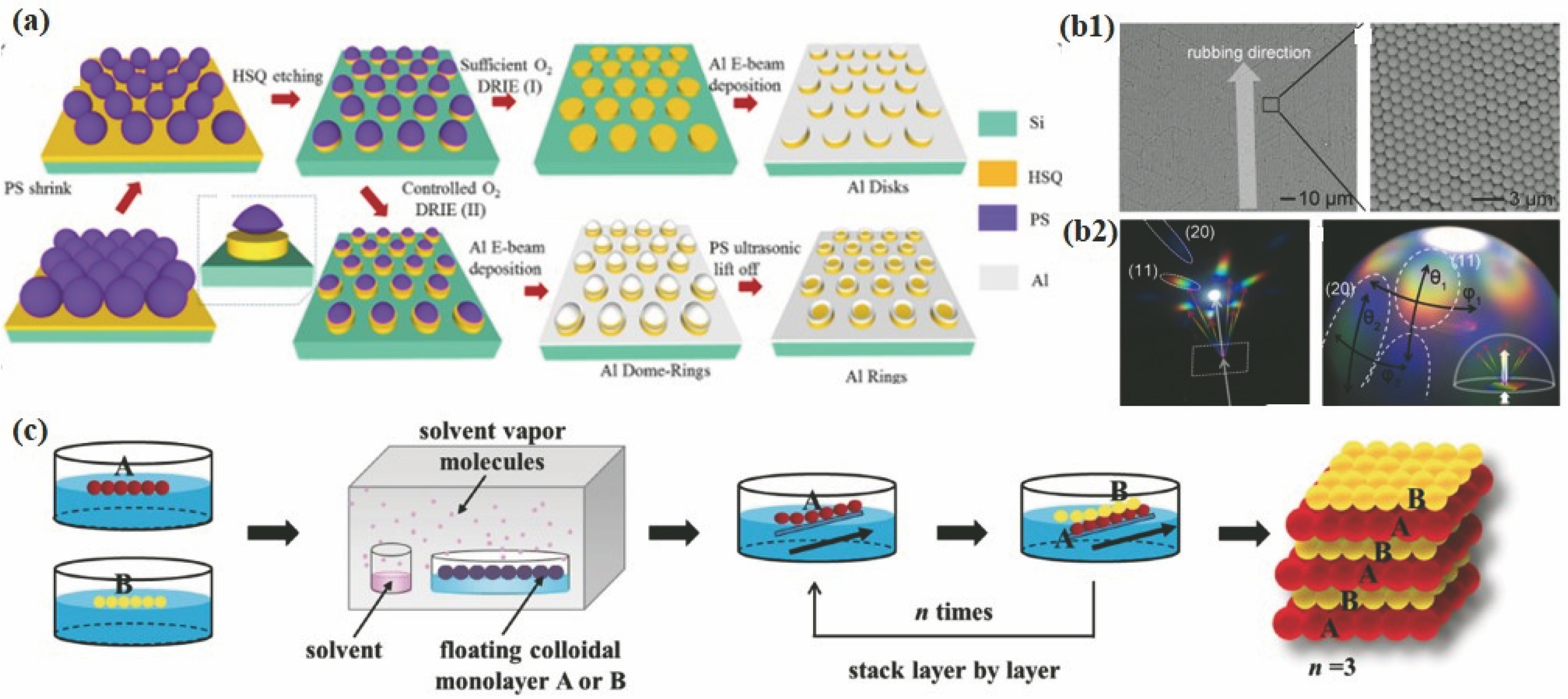
![Fabrication process for changing structural color or photonic band gap. (a) Schematic of fabrication processes of disk and ring structures[33]; (b1) scanning electron microscope (SEM) images of PS nanosphere after rubbing on PDMS-coated glass slide[34]; (b2) different colors depended on tilted angle (θ), azimuthal angle (Q), and sample-to-eye distance[<xref r](/richHtml/lop/2019/56/23/230001/img_1.jpg)
Fig. 1. Fabrication process for changing structural color or photonic band gap. (a) Schematic of fabrication processes of disk and ring structures[33]; (b1) scanning electron microscope (SEM) images of PS nanosphere after rubbing on PDMS-coated glass slide[34]; (b2) different colors depended on tilted angle (θ ), azimuthal angle (Q ), and sample-to-eye distance[![Fabrication processes related to color printing. (a1) Schematic of printing process using inkjet printer[36]; (a2) diffraction spectra with incident angle θi=60°[36]; (a3) reflectivity of light with different wavelengths at different incident angles[36]; (b) schematic of “drop-casting” procedure[<xref ref-type="bibr](/richHtml/lop/2019/56/23/230001/img_2.jpg)
![Fabrications related to color printing. (a) Schematic of fabrication process of sandwich structure using freestanding photonic crystal film[40]; (b) schematic of self-assembled ACAs[41]; (c) schematic of inkjet printing process of CdS pattern on paper-based substrates[42]; (d1) (d2) schematics of fabrication processes of colloidal crystal patterns<](/Images/icon/loading.gif)
![Holograms of opal-like structures formed on different substrates under different incident angles. (a)-(c) Silicon wafer; (d) (e) glass slide; (f) (g) glossy photo paper[44]](/Images/icon/loading.gif)
![Fabrication processes related to anti-reflective coating. (a) Sample of UT-SOI and fabrication process[46]; (b) fabrication process of TiO2 layer[47]; (c1) schematic of ideal plasmonic absorber[48]; (c2) self-assembly of gold nanoparticles to form plasmonic absorbers[48]; (c3) images of n](/Images/icon/loading.gif)
![Structure and luminous efficiency of LEDs. (a1) Principle of InGaN quantum well LED[50]; (a2) light output power as a function of current for InGaN quantum well LED [50]; (b1) schematic of LED bottom reflector with superlattice[35]; (b2) (b3) light output power and electro-luminescence spectra[35]](/Images/icon/loading.gif)
![Fabrication of microlens arrays. (a) Schematic of mass production of microlens array by nanosphere lithography[55]; (b1) diffraction image of fabricated 4-inch glass substrate coated with PS nanosphere mask[55]; (b2)-(b4) optical microscope images of microlens array at different observation scales[55]; (c1) simulated light-field distribution[<](/Images/icon/loading.gif)
![Colloidal-crystal laser. (a) Principle of low-threshold colloidal-crystal laser[56]; (b) schematics of photonic band gap shift under voltages in different bias directions[57]](/Images/icon/loading.gif)
![Fabrication process of sensors. (a) Micro-nano fabrication process flow of bio-inspired Si3N4-membrane[65]; (b) schematic of self-assembly process and SEM image of fiber end[66]; (c) schematic of Raman measurement[67]](/Images/icon/loading.gif)
![Self-assembled molecular-colloidal motor. (a) Three-dimensional schematic of self-assembled molecular-colloidal light-driven motor. Rods in xz plane represent liquid crystal molecules and, and rods in xy plane represent azobenzene molecules[68]; (b) snapshots of translational motion of platelet under polarized blue light and polarized white light[68]](/Images/icon/loading.gif)
![Fabrication processes related to color printing. (a1) Schematic of printing process using inkjet printer[36]; (a2) diffraction spectra with incident angle θi=60°[36]; (a3) reflectivity of light with different wavelengths at different incident angles[36]; (b) schematic of “drop-casting” procedure[<xref ref-type="bibr](/richHtml/lop/2019/56/23/230001/img_2.jpg)
Fig. 2. Fabrication processes related to color printing. (a1) Schematic of printing process using inkjet printer[36]; (a2) diffraction spectra with incident angle θ i=60°[36]; (a3) reflectivity of light with different wavelengths at different incident angles[36]; (b) schematic of “drop-casting” procedure[Download full size
Fig. 3. Fabrications related to color printing. (a) Schematic of fabrication process of sandwich structure using freestanding photonic crystal film[40]; (b) schematic of self-assembled ACAs[41]; (c) schematic of inkjet printing process of CdS pattern on paper-based substrates[42]; (d1) (d2) schematics of fabrication processes of colloidal crystal patterns<
Fig. 4. Holograms of opal-like structures formed on different substrates under different incident angles. (a)-(c) Silicon wafer; (d) (e) glass slide; (f) (g) glossy photo paper[44]
Fig. 5. Fabrication processes related to anti-reflective coating. (a) Sample of UT-SOI and fabrication process[46]; (b) fabrication process of TiO2 layer[47]; (c1) schematic of ideal plasmonic absorber[48]; (c2) self-assembly of gold nanoparticles to form plasmonic absorbers[48]; (c3) images of n
Fig. 6. Structure and luminous efficiency of LEDs. (a1) Principle of InGaN quantum well LED[50]; (a2) light output power as a function of current for InGaN quantum well LED [50]; (b1) schematic of LED bottom reflector with superlattice[35]; (b2) (b3) light output power and electro-luminescence spectra[35]
Fig. 7. Fabrication of microlens arrays. (a) Schematic of mass production of microlens array by nanosphere lithography[55]; (b1) diffraction image of fabricated 4-inch glass substrate coated with PS nanosphere mask[55]; (b2)-(b4) optical microscope images of microlens array at different observation scales[55]; (c1) simulated light-field distribution[<
Fig. 8. Colloidal-crystal laser. (a) Principle of low-threshold colloidal-crystal laser[56]; (b) schematics of photonic band gap shift under voltages in different bias directions[57]
Fig. 9. Fabrication process of sensors. (a) Micro-nano fabrication process flow of bio-inspired Si3N4-membrane[65]; (b) schematic of self-assembly process and SEM image of fiber end[66]; (c) schematic of Raman measurement[67]
Fig. 10. Self-assembled molecular-colloidal motor. (a) Three-dimensional schematic of self-assembled molecular-colloidal light-driven motor. Rods in xz plane represent liquid crystal molecules and, and rods in xy plane represent azobenzene molecules[68]; (b) snapshots of translational motion of platelet under polarized blue light and polarized white light[68]

Set citation alerts for the article
Please enter your email address


