• Photonics Research
  • Vol. 9, Issue 10, 2006 (2021)
Ying Zhang1、†, Qiang Liu1、†, Chenyang Mei, Desheng Zeng, Qingzhong Huang*, and Xinliang Zhang
Author Affiliations
  • Wuhan National Laboratory for Optoelectronics, Huazhong University of Science and Technology, Wuhan 430074, China
  • show less
    DOI: 10.1364/PRJ.434151 Cite this Article Set citation alerts
    Ying Zhang, Qiang Liu, Chenyang Mei, Desheng Zeng, Qingzhong Huang, Xinliang Zhang. Proposal and demonstration of a controllable Q factor in directly coupled microring resonators for optical buffering applications[J]. Photonics Research, 2021, 9(10): 2006 Copy Citation Text show less
    (a) Schematic configuration of the Q-factor controllable structure. (b) Transmission spectra at the through port with/without refractive index change, illustrating the variation of Δλ; inset: zoom-in of the spectra around λ0. Optical intensities in Ring 1 and Ring 2 (c) before tuning and (d) after tuning.
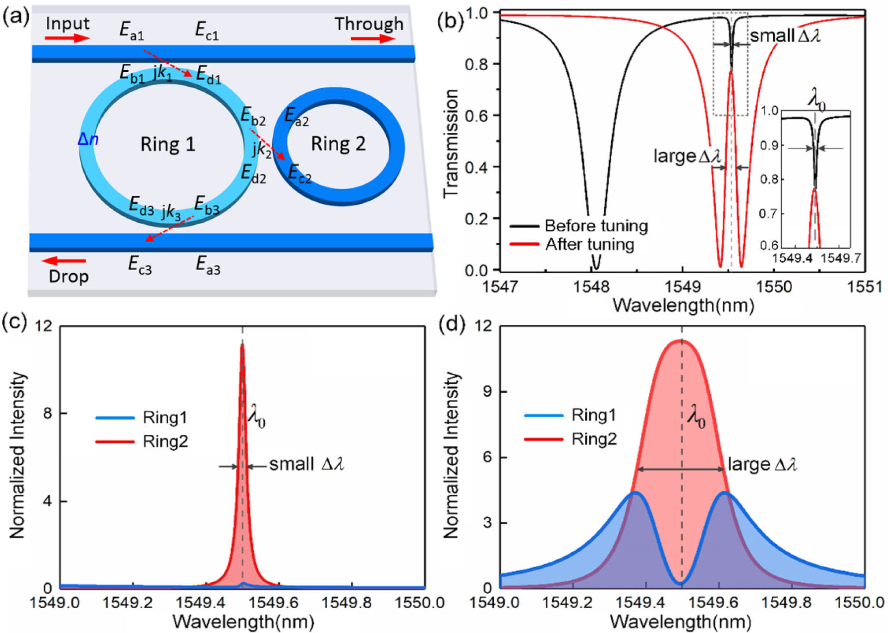
    Fig. 1. (a) Schematic configuration of the Q-factor controllable structure. (b) Transmission spectra at the through port with/without refractive index change, illustrating the variation of Δλ; inset: zoom-in of the spectra around λ0. Optical intensities in Ring 1 and Ring 2 (c) before tuning and (d) after tuning.
    (a) Microscope image of the fabricated Q-factor controllable system. (b) Scanning electron microscopy images of different coupling regions before the SiO2 layer was deposited. (c) Schematic of waveguide cross section in Ring 1 with a Ti heater on the top.
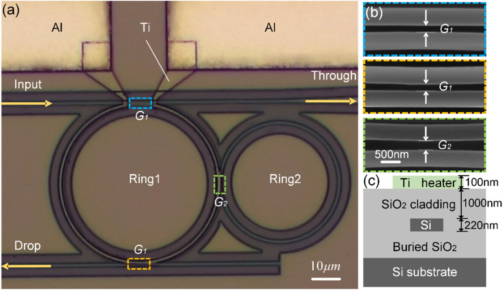
    Fig. 2. (a) Microscope image of the fabricated Q-factor controllable system. (b) Scanning electron microscopy images of different coupling regions before the SiO2 layer was deposited. (c) Schematic of waveguide cross section in Ring 1 with a Ti heater on the top.
    (a) Experimental transmission spectra (circle dots) and theoretical fits (solid curves) of the fabricated device. Inset: zoom-in of the high-Q resonance. (b) Normalized intensity in Ring 2 theoretically simulated using the fitting parameters.
    Fig. 3. (a) Experimental transmission spectra (circle dots) and theoretical fits (solid curves) of the fabricated device. Inset: zoom-in of the high-Q resonance. (b) Normalized intensity in Ring 2 theoretically simulated using the fitting parameters.
    (a) Experimental transmission spectra (circle dots) and theoretical fits (solid curves) of the fabricated device with G2 of 160 nm. (b) Normalized intensity in Ring 2 theoretically simulated using the fitting parameters.
    Fig. 4. (a) Experimental transmission spectra (circle dots) and theoretical fits (solid curves) of the fabricated device with G2 of 160 nm. (b) Normalized intensity in Ring 2 theoretically simulated using the fitting parameters.
    Experimental transmission spectra (circle dots) and theoretical fits (solid curves) of the devices with different G2 in the (a) low-Q state and (b) high-Q state.
    Fig. 5. Experimental transmission spectra (circle dots) and theoretical fits (solid curves) of the devices with different G2 in the (a) low-Q state and (b) high-Q state.
    Normalized intensity spectra in Ring 2 for different k2 ranging from 0.12 to 0.39.
    Fig. 6. Normalized intensity spectra in Ring 2 for different k2 ranging from 0.12 to 0.39.
    (a) Time delay of the system as a function of wavelength detuning in the high-Q state and low-Q state, theoretically simulated using the extracted parameter values of the device shown in Fig. 3. The maximum time delay and time advance are provided at points P1 and P2, respectively. (b) The measured optical pulses output from the system in the low-Q state (P1) and reference waveguide (R). The time delay is obtained by comparing the two pulses in the time domain. (c) The measured phase shift response (red circles) and its fitting curve (red line) of the system in the high-Q state. The time delay (black line) is deduced from the fitted phase shift using τd =−dφ/dω. (d) The time delay and FWHM (Δλ) of the system in the low-Q state and high-Q state for different G2. The system produces slow light and fast light (time delay having negative values) in the low-Q state and high-Q state, respectively.
    Fig. 7. (a) Time delay of the system as a function of wavelength detuning in the high-Q state and low-Q state, theoretically simulated using the extracted parameter values of the device shown in Fig. 3. The maximum time delay and time advance are provided at points P1 and P2, respectively. (b) The measured optical pulses output from the system in the low-Q state (P1) and reference waveguide (R). The time delay is obtained by comparing the two pulses in the time domain. (c) The measured phase shift response (red circles) and its fitting curve (red line) of the system in the high-Q state. The time delay (black line) is deduced from the fitted phase shift using τd=dφ/dω. (d) The time delay and FWHM (Δλ) of the system in the low-Q state and high-Q state for different G2. The system produces slow light and fast light (time delay having negative values) in the low-Q state and high-Q state, respectively.
    Simulated dynamics of the intra-cavity and output optical intensities of the system under control. (a) Normalized intensity in Ring 1/Ring 2 with S control (storing at t=65 ps, dashed lines), or S+R control (storing at t=65 ps and releasing at t=100 ps, solid lines). When Ring 1 is dynamically tuned by S control, the system is immediately switched to the high-Q state and stores light in Ring 2. Then, as R control is applied, the system returns to the low-Q state and releases light from Ring 2. (b) Optical intensities at the output ports (through: solid lines; drop: dashed lines) with S+R control (storing at t=65 ps, different releasing time). When S control is applied, the pulse intensities at the output ports become low, since the light is trapped in Ring 2. (c) Optical intensities at the output ports (through: solid lines; drop: dashed lines) of different systems, whose curves are offset for clarity. S control is applied for storing, just when the optical intensity in Ring 2 reaches the maximum. (d) The peak intensity of output pulse at the drop port as a function of storage time. The system denoted by k2=0.10 is identical to that in Fig. 3, while the systems denoted by k2=0.12, 0.17, 0.24, 0.31, 0.39 are identical to those in regions (i)–(v) in Fig. 5, respectively, except for the slow tuning. Here, these systems are assumed to be dynamically tunable.
    Fig. 8. Simulated dynamics of the intra-cavity and output optical intensities of the system under control. (a) Normalized intensity in Ring 1/Ring 2 with S control (storing at t=65  ps, dashed lines), or S+R control (storing at t=65  ps and releasing at t=100ps, solid lines). When Ring 1 is dynamically tuned by S control, the system is immediately switched to the high-Q state and stores light in Ring 2. Then, as R control is applied, the system returns to the low-Q state and releases light from Ring 2. (b) Optical intensities at the output ports (through: solid lines; drop: dashed lines) with S+R control (storing at t=65  ps, different releasing time). When S control is applied, the pulse intensities at the output ports become low, since the light is trapped in Ring 2. (c) Optical intensities at the output ports (through: solid lines; drop: dashed lines) of different systems, whose curves are offset for clarity. S control is applied for storing, just when the optical intensity in Ring 2 reaches the maximum. (d) The peak intensity of output pulse at the drop port as a function of storage time. The system denoted by k2=0.10 is identical to that in Fig. 3, while the systems denoted by k2=0.12, 0.17, 0.24, 0.31, 0.39 are identical to those in regions (i)–(v) in Fig. 5, respectively, except for the slow tuning. Here, these systems are assumed to be dynamically tunable.
    MechanismStructureMaterialControl MethodQ Tuning RangeReference
    Control of loss/couplingPhC cavitySi-SiO2AO tuning, off chip52,000–210,000[18]
    MRR integrated with an SOAInP-InGaAsPElectrical pumping, on chip13,000–32,000a[19]
    MRR coupled with a waveguideSi-SiO2TO tuning, on chip9000–96,000[20]
    Interference between a resonator and a feedback waveguideMRR with interferometric couplersSi-SiO2TO tuning, on chip2200–15,500[14]
    PhC cavity–waveguide–mirror systemSi-SiO2AO tuning, off chip3000–12,000[21]
    PhC cavity–waveguide–mirror systemSi-SiO2AO tuning, off chip3800–22,000[22]
    PhC cavity–waveguide–mirror systemGaAs-AlGaAsAO tuning, off chip7900–40,000[23]
    Interference between coupled resonatorsTwo indirectly coupled MRRsSi-SiO2EO tuning, on chip6000–20,000[24]
    Two indirectly coupled MRRsSi-SiO2AO tuning, off chip23,000–53,000b[17]
    Laterally coupled vertical cavitiesGaAs-AlGaAsTO tuning, off chip1650–1900[34]
    Two directly coupled MRRsSi-SiO2TO tuning, on chip16,400–56,5002800–21,800Our work
    Table 1. Comparison of Various Q-Factor Controllable Systems
    Ying Zhang, Qiang Liu, Chenyang Mei, Desheng Zeng, Qingzhong Huang, Xinliang Zhang. Proposal and demonstration of a controllable Q factor in directly coupled microring resonators for optical buffering applications[J]. Photonics Research, 2021, 9(10): 2006
    Download Citation