• Photonics Research
  • Vol. 9, Issue 10, 2006 (2021)
Ying Zhang1、†, Qiang Liu1、†, Chenyang Mei, Desheng Zeng, Qingzhong Huang*, and Xinliang Zhang
Author Affiliations
  • Wuhan National Laboratory for Optoelectronics, Huazhong University of Science and Technology, Wuhan 430074, China
  • show less
    DOI: 10.1364/PRJ.434151 Cite this Article Set citation alerts
    Ying Zhang, Qiang Liu, Chenyang Mei, Desheng Zeng, Qingzhong Huang, Xinliang Zhang. Proposal and demonstration of a controllable Q factor in directly coupled microring resonators for optical buffering applications[J]. Photonics Research, 2021, 9(10): 2006 Copy Citation Text show less

    Abstract

    Optical resonators with controllable Q factors are key components in many areas of optical physics and engineering. We propose and investigate a Q-factor controllable system composed of two directly coupled microring resonators, one of which is tunable and coupled to dual waveguides. By shifting the resonance of the controllable microring, the Q factor of the system as well as the other microring changes significantly. We have demonstrated wide-range controllable Q factors based on this structure in silicon-on-insulator, for example. The influences of spectral detuning and coupling strength between two resonators on the variation of Q factors are studied in detail experimentally. Then, we explore its applications in optical buffering. Tunable fast-to-slow/slow-to-fast light has been carried out by switching the system between the high-Q state and low-Q state. Moreover, optical pulse capture and release are also achievable using this structure with dynamic tuning, and the photon storage properties are investigated. The proposed Q-factor tunable system is simple, flexible, and realizable in various integrated photonic platforms, allowing for potential applications in on-chip optical communications and quantum information processing.

    1. INTRODUCTION

    Optical resonators [1] have been widely used in various devices, such as light sources [2,3], filters [4,5], modulators [6,7], switches [8,9], and buffers [1012], which are essential components for optical communications and optical signal processing. As a characteristic parameter, the Q factor of resonators is a measure of the sharpness of a resonant peak, or the strength of the damping of a resonating mode. The Q factor is inversely proportional to the bandwidth, and proportional to the photon lifetime. Control of the Q factor is meaningful and allows for the applications in Q-switched lasers [13], bandwidth-tunable filters [14], tunable modulators [15], tunable time delay lines [16], and stopping light devices [17]. Based on a microring resonator (MRR) with a tunable Q factor, a silicon filter has been demonstrated with continuously tunable bandwidth [14], which is required in reconfigurable optical add–drop multiplexing systems. Similarly, by changing the Q factor through tunable interferometric couplers, Liu et al. realized a multi-ring resonator-based delay line with tunable time delay and bandwidth [16], and then applied it in the 1×4 optical beamforming networks. In addition, optical pulse can be stored and released in a Q-factor controllable structure [17], overcoming the delay-bandwidth limit, when the tuning is within a time scale shorter than the photon lifetime of the resonator.

    To date, there are fundamentally three approaches to control the Q factor. First, the Q factor is tuned by directly changing the intrinsic loss in the resonator or coupling coefficient between the waveguide and the resonator [1820]. Through pumping the photonic crystal (PhC) nanocavity with a short pulse, numerous free carriers are generated in the cavity and bring significant absorption loss, resulting in the change of Q factor [18]. Alternatively, by tuning the coupling coefficient of a 2×2 directional coupler, an MRR exhibited a controllable Q factor between 9000 and 96,000 [19]. However, in these cases, the central wavelength shifts greatly as the Q factor changes. Second, the Q factor is controlled by adjusting the phase shift in the feedback coupled waveguide(s) [14,2123]. A ring resonator with tunable bandwidth from 0.1 to 0.7 nm, corresponding to a Q factor from 15,500 to 2200, is realized by thermal-optic (TO) tuning of the phase shift in the interferometric couplers [14]. Another structure is the PhC cavity–waveguide–mirror system, where the interference between light coupled out from the cavity and light reflected back from the mirror determines the Q factor [2123]. A tunable Q factor from 3000 to 12,000 has been achieved [21], as the phase shift in the feedback waveguide is all-optically changed. Nevertheless, this approach needs phase shift change as large as π and relatively high power consumption. Third, the control of the Q factor is implemented by detuning the indirectly coupled two resonators, which exhibit an electromagnetically induced transparency (EIT)-like effect [17,24]. Previously, the Q factor of EIT-like resonance has been tuned from 6000 to 20,000 by electro-optic (EO) control [24], and from 23,000 to 53,000 by all-optical (AO) control [17]. However, the reported EIT-like systems have stringent fabrication requirements, in demand of two nearly identical resonators with an optimized distance.

    In this paper, we present and investigate systematically a Q-factor tunable system comprising a dual-waveguide coupled tunable MRR, which is also directly coupled to another MRR [25]. Previously, similar structures [26,27] have been presented and employed for cross-connect filters, switches, and modulators, whereas here we modify and apply it to construct a Q-factor tunable system for the first time. By controlling one MRR, the Q factors of the system and the other MRR both change significantly. The system exhibits an EIT-like resonance with a low Q factor, when the two resonators are spectrally aligned. In contrast, the system behaves like a notch filter with a high Q factor, when the two resonators are adequately detuned by varying the phase shift (much lower than π) in the controllable resonator. During the tuning of one resonator, the peak transmission can keep low loss, and the central wavelength of the resonant mode is nearly maintained, since the other resonator with a high Q factor is not tuned. It makes the system quite appropriate for optical buffering. The proposed Q-factor controllable system is theoretically analyzed, and then demonstrated on a silicon-on-insulator platform. The dependence of Q-factor tunability on the structural parameters has been studied in detail in experiment. After that, we apply this device in optical buffering. Fast-to-slow/slow-to-fast light has been realized by adjusting the Q factor. Furthermore, the potential applications of such a device in stopping, storing, and releasing light are also investigated, assuming ultra-fast tuning of the resonator. Due to the high performance, the proposed system will find applications in on-chip optical communications, optical interconnect, and optical signal processing.

    2. DEVICE STRUCTURE AND THEORY

    Figure 1(a) shows a schematic configuration of the presented Q-factor controllable system. It consists of a two-bus symmetrically coupled MRR (Ring 1), which is also directly coupled to another MRR (Ring 2). Here, Ring 1 is controllable by changing the refractive index of the waveguide, while Ring 2 is fixed. Using the transfer matrix method, the relations of E-fields at different positions labeled in Fig. 1(a) are given by Eci=tiEai+jkiEbi,i=1,2,3,Edi=tiEbi+jkiEai,i=1,2,3,Eb2=α11/4Ed1exp(jδ1/4),Eb3=α11/4Ed2exp(jδ1/4),Eb1=α11/2Ed3exp(jδ1/2),Ea2=α2Ec2exp(jδ2),where ki and ti (i=1,2,3) represent the field coupling coefficient and transmission coefficient, respectively, satisfying ki2+ti2=1 and k1=k3; and α1(α2) and δ1(δ2) denote the round-trip field attenuation and phase shift in Ring 1 (Ring 2), respectively. For simplicity, all the waveguides in our structure are considered to have the same cross-sectional dimensions and mode effective index neff. Then, the round-trip phase shifts satisfy δ1=4π2R1(neff+Δn)/λ and δ2=4π2R2neff/λ, where Δn is the change of the mode effective index in Ring 1, λ is vacuum wavelength, and R1 (R2) is the radius of Ring 1 (Ring 2).

    (a) Schematic configuration of the Q-factor controllable structure. (b) Transmission spectra at the through port with/without refractive index change, illustrating the variation of Δλ; inset: zoom-in of the spectra around λ0. Optical intensities in Ring 1 and Ring 2 (c) before tuning and (d) after tuning.

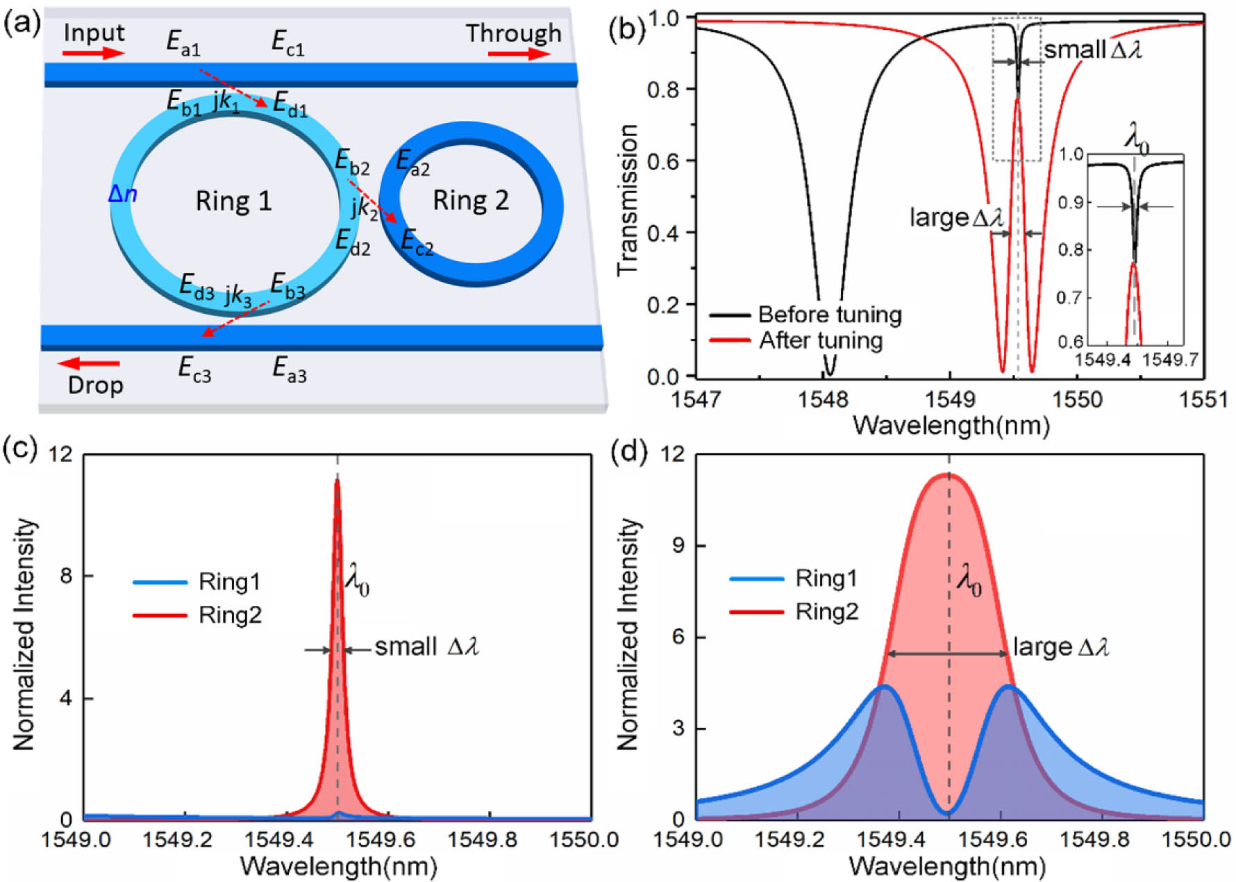
    Figure 1.(a) Schematic configuration of the Q-factor controllable structure. (b) Transmission spectra at the through port with/without refractive index change, illustrating the variation of Δλ; inset: zoom-in of the spectra around λ0. Optical intensities in Ring 1 and Ring 2 (c) before tuning and (d) after tuning.

    Consequently, the transfer functions at the through port (St=Ec1/Ea1) and drop port (Sd=Ec3/Ea1) of the system are deduced as St=t1α1t1τ21exp(jδ1)1α1τ21t12exp(jδ1),Sd=α11/2τ21k12exp(jδ1/2)1α1τ21t12exp(jδ1),where τ21=[t2α2exp(jδ2)]/[1α2t2exp(jδ2)] is the transfer function of the waveguide section in Ring 1 coupled to Ring 2. Hence, the power transmission at the through port and drop port can be given by |St|2 and |Sd|2, respectively. These expressions are simple and convenient for us to analyze the response spectrum and extract the Q factor of the system. Combining Eqs. (1) and (2), we can gain more insight into the behavior of the system. The normalized intensities in Ring 1 (I1=|Ed1/Ea1|2) and Ring 2 (I2=|Ec2/Ea1|2) are described by I1=|k1[1α2t2exp(jδ2)]1α2t2exp(jδ2)α1t12exp(jδ1)[t2α2exp(jδ2)]|2,I2=α11/2k12k22|1α2t2exp(jδ2)α1t12exp(jδ1)[t2α2exp(jδ2)]|2.

    To analyze this system, we have calculated the transmission spectra at the output port using the previous equations. There are some basic considerations to choose parameter values. First, Ring 1 is designed as a low-Q resonator with a large extinction ratio. Hence, we need relatively strong coupling between Ring 1 and bus waveguides. The loss in Ring 1 is relatively large, since the added structure (e.g., metal heater, PN junction) for control may cause more loss. Second, Ring 2 is designed as a high-Q resonator, so the coupling between Ring 2 and Ring 1 is relatively weak and the loss in Ring 2 is low. In our design, the radius of Ring 2 is smaller than that of Ring 1, and thus the coupling between bus waveguides and Ring 2 is negligible due to the large spacing gap. In fact, there is no tight constraint on the radius difference between Ring 1 and Ring 2. As an example, we set the parameters as R1=28.0  μm, R2=21.0  μm, neff=2.7445, k1=0.44, k2=0.13, α1=0.95, and α2=0.99, which are also generally consistent with the experimental results in the following sections. It is known that the Q factor is equal to λ0/Δλ, where λ0 is the central wavelength and Δλ is the full width at half-maximum (FWHM). By controlling Ring 1, the Q factors of the system and Ring 2 both change significantly. When the MRRs are greatly detuned, Δλ is the FWHM of the high-Q resonant valley. Then, as the MRRs are aligned, Δλ is the FWHM of the low-Q EIT resonance. In previous works [24,28], the definition of the Q factor of such hybrid modes (i.e., EIT modes) has been provided and the controllable Q factor in an EIT system has ever been investigated.

    Figure 1(b) shows the transmission spectra at the through port before and after the tuning of Δn=2.6×10³. Without tuning, the transmission spectrum exhibits a nearly Lorentzian line shape around the central wavelength, with a FWHM of 24 pm and a corresponding Q factor of 64,600. The broad resonant valley of Ring 1 and narrow resonant valley of Ring 2 are distinctly separated. In contrast, after tuning, the resonances of two rings are aligned and strongly interfere. The transmission exhibits an EIT-like line shape, with an FWHM of 117 pm and a corresponding Q factor of 13,300. During the tuning process, the resonance of Ring 1 shifts by 1.473 nm, corresponding to a phase shift variation of 0.6π in Ring 1. Note that the Q factor of the system is reduced about 5 times after the refractive index tuning. Then, the central wavelength (λ0) is generally maintained, and the valley (peak) transmission is still low loss for the high-Q Lorentzian resonance and low-Q EIT resonance. Moreover, the optical power is mainly localized in Ring 2 of the system either in the high-Q or low-Q state. Note that when Ring 2 is tuned instead, the Q factors of the system and Ring 2 also change, but the central wavelength (λ0) of resonance is shifted greatly, which is not desired for optical buffering.

    To provide more insight, we have further calculated the optical intensities in Ring 1 and Ring 2 before and after tuning. Figures 1(c) and 1(d) illustrate the variation of internal optical intensity in Ring 2 after tuning, illustrating the controllable Q factor of Ring 2. The internal intensity spectrum in Ring 2 can be characterized by measuring the emitted light from Ring 2 to the free space [21,22]. As shown in Fig. 1(c), before tuning, Ring 2 is on-resonance, while Ring 1 is off-resonance, indicating that the power in Ring 2 escaping to bus waveguides is hindered. The intensity spectrum exhibits an FWHM of 24 pm and a corresponding Q factor of 64,600 for Ring 2. The situation becomes different after tuning. Figure 1(d) shows that when the two rings both are on-resonance, the interference causes the substantial reduction of fields in Ring 1 around the central wavelength, which is nearly fixed due to the unchanged Ring 2. Then, the intensity spectrum exhibits an FWHM of 233 pm and a corresponding Q factor of 6700 for Ring 2. The significant Q-factor change (nearly 10 times) allows for light storing and releasing in Ring 2 with an ultra-fast tuning. From those results, we know that the increase/decrease of Q factors of the system and Ring 2 is easily controllable by just tuning Ring 1. It is noteworthy that the structure can be implemented on various material platforms, such as silicon-on-insulator, silicon nitride [29], lithium niobate-on-insulator [30], and AlGaAs-on-insulator [31]. Moreover, the tunability of the system can be realized via different mechanisms, such as TO effect, EO effect, acousto-optical effect, and Kerr effect.

    3. EXPERIMENTAL RESULTS

    A. Device Fabrication

    A proposed structure was fabricated on a silicon-on-insulator platform for example, as shown in Fig. 2. The top silicon layer and buried oxide layer are 220 nm and 2 μm in thickness, respectively. The waveguides and rings were all defined using e-beam lithography, followed by inductively coupled plasma etching. Simultaneously, grating couplers were constructed to couple the device with input/output fiber for TE polarization. The straight and bent waveguides all have a height of 220 nm and a width of 450 nm. The radii of Ring 1 and Ring 2 are about 28 μm and 21 μm, respectively. The spacing gap between Ring 1 and waveguide (Ring 2) is G1=200  nm (G2=300  nm), as illustrated in Fig. 2(b). Then, a 1 μm thick SiO2 layer was deposited on the surface by plasma-enhanced chemical vapor deposition. After that, we patterned the metal heaters using e-beam lithography, e-beam evaporation, and lift-off techniques. The Ti heater of 100 nm in thickness and 1 μm in width was placed on top of Ring 1 for thermal tuning, as seen in Fig. 2(c). Finally, Al contact pads with a thickness of 1 μm were patterned in the same way as the Ti heater.

    (a) Microscope image of the fabricated Q-factor controllable system. (b) Scanning electron microscopy images of different coupling regions before the SiO2 layer was deposited. (c) Schematic of waveguide cross section in Ring 1 with a Ti heater on the top.

    Figure 2.(a) Microscope image of the fabricated Q-factor controllable system. (b) Scanning electron microscopy images of different coupling regions before the SiO2 layer was deposited. (c) Schematic of waveguide cross section in Ring 1 with a Ti heater on the top.

    B. Control of Q Factor

    Figure 3(a) illustrates the normalized transmission spectra of the fabricated device at the through port for different heating powers. In the beginning, without heating, the transmission spectrum exhibits two separated valleys. The left resonant valley from Ring 1 is broadband and has a high extinction ratio. In contrast, the right valley from Ring 2 has an FWHM of only 27 pm, corresponding to a Q factor of 56,500, and the transmission loss is 2.2 dB at the central wavelength. As the heating power increases, the resonances of Ring 1 and Ring 2 become closer. When the power is 9.04 mW, the resonances of two rings are aligned, and we obtain an EIT-like response, with an FWHM of 94 pm, corresponding to a Q factor of 16,400, and a transmission loss of 1.8 dB at the central wavelength. During this process, the central wavelength of interest is slightly redshifted by 0.08 nm, which is mostly attributed to the fact that Ring 2 is partly heated by the nearby heater on Ring 1 in the coupling region. After all, in this case, as Ring 1 is controlled, this system changes between the high-Q state (notch filtering) and low-Q state (EIT-like transmission), and still maintains low loss for the central wavelength. The measured spectra given in Fig. 3(a) are well explained by the theoretical modeling with the fitting parameters: α1=0.95, α2=0.99, k1=0.42, k2=0.10, and different Δn for a corresponding heating power (e.g., Δn=1.15×10³ for 9.04 mW power). The theoretical fit agrees very well with the experimental measurement. Using the fitting parameters, we have calculated the normalized intensity in Ring 2, as shown in Fig. 3(b), corresponding to the transmission in Fig. 3(a). It is found that the intensity spectrum has a Lorentzian line shape, and the Q factor of Ring 2 is tunable between 49,200 and 12,000 during the tuning process.

    (a) Experimental transmission spectra (circle dots) and theoretical fits (solid curves) of the fabricated device. Inset: zoom-in of the high-Q resonance. (b) Normalized intensity in Ring 2 theoretically simulated using the fitting parameters.

    Figure 3.(a) Experimental transmission spectra (circle dots) and theoretical fits (solid curves) of the fabricated device. Inset: zoom-in of the high-Q resonance. (b) Normalized intensity in Ring 2 theoretically simulated using the fitting parameters.

    To further study the Q factor control, we fabricated and characterized another device with only a changed G2 of 160 nm. Figure 4 shows that the system varies from the high-Q state to the low-Q state and then back to the high-Q state, as the heating power increases and the resonance of Ring 1 is redshifted continuously. In the beginning, the resonance of Ring 2 is on the right side and far from the resonance of Ring 1. The dual-MRR system exhibits a high-Q resonance (Q=30,500) around the resonant wavelength of Ring 2, as seen in region (i) in Fig. 4(a). Then, when the power is increased to 9.40 mW, the two resonances of Ring 1 and Ring 2 are aligned, and the system shows a low-Q EIT resonance (Q=4600) arising from the interference between two resonating modes of MRRs, as plotted in region (ii) in Fig. 4(a). Finally, when the power is 19.29 mW, the resonance of Ring 1 is shifted to the right side, and the system returns to the high-Q state (Q=31,100), as seen in region (iii) in Fig. 4(a). The transmission spectra of system between the high-Q state and low-Q state exhibit asymmetric Fano line shapes, which are similar to those shown in Fig. 3 and not provided here. These results are basically consistent with the prior works [32,33]. The fitting curves are consistent with the experimental results, as seen in Fig. 4(a), and the fitting parameters are given by k1=0.44, k2=0.28, α1=0.97, α2=0.99, and different Δn. Using these values, the optical intensities in Ring 2 for different heating powers have been calculated, as illustrated in Fig. 4(b). It is observed that the optical intensity becomes a broadband and weakly resolved doublet, no longer showing a Lorentzian line shape. In this case, the extracted low Q factor of Ring 2 is quite different from that of the system. Moreover, the intensity enhancement in Ring 2 changes substantially as the Q factor is tuned, implying potential nonlinear optical applications of this system.

    (a) Experimental transmission spectra (circle dots) and theoretical fits (solid curves) of the fabricated device with G2 of 160 nm. (b) Normalized intensity in Ring 2 theoretically simulated using the fitting parameters.

    Figure 4.(a) Experimental transmission spectra (circle dots) and theoretical fits (solid curves) of the fabricated device with G2 of 160 nm. (b) Normalized intensity in Ring 2 theoretically simulated using the fitting parameters.

    Figures 5(a) and 5(b) show the measured transmission spectra of the system with a changed G2 ranging from 150 nm to 300 nm in the low-Q state and high-Q state, respectively. We obtain the Q factor and extinction ratio from the experimental transmission spectra. It is found that, in the low-Q state, the Q factor increases from 2800 to 17,000, and the central transmission loss increases from 0.03 dB to 1.1 dB, as G2 increases. On the other side, in the high-Q state, the Q factor increases from 21,800 to 51,700, while the central transmission loss decreases from 5.2 dB to 1.8 dB, as G2 increases. The theoretical curves are also given and fit the measured spectra well. In Fig. 5(b), regions (i) and (ii), these high-Q resonances are not so sharp and symmetric. We attribute it to the fabrication imperfection and the possible optical backscattering in the high-Q MRR (i.e., Ring 2), which will broaden the resonant valley and decrease the extinction ratio.

    Experimental transmission spectra (circle dots) and theoretical fits (solid curves) of the devices with different G2 in the (a) low-Q state and (b) high-Q state.

    Figure 5.Experimental transmission spectra (circle dots) and theoretical fits (solid curves) of the devices with different G2 in the (a) low-Q state and (b) high-Q state.

    The coupling coefficient k2 is extracted for each G2, as denoted in Fig. 5(b). Then, we can speculate the normalized intensity spectra in Ring 2. As shown in Fig. 6, for a small k2, the normalized intensity shows a single peak, which is strong and narrowband. As k2 increases gradually from 0.12 to 0.39, the single peak becomes broadband and flattop at first, then splits into a weakly resolved doublet, and finally becomes a widely spaced doublet. At the same time, we find that the power enhancement in Ring 2 at the central wavelength decreases continuously.

    Normalized intensity spectra in Ring 2 for different k2 ranging from 0.12 to 0.39.

    Figure 6.Normalized intensity spectra in Ring 2 for different k2 ranging from 0.12 to 0.39.

    Table 1 summarizes and compares the existing Q-factor controllable systems, which are classified into three types according to the mechanisms. Changing the resonator’s loss or coupling to waveguide is a direct and simple approach, and a controllable Q factor with a large tuning range has been obtained. However, the central wavelength shifts greatly (e.g., >1.5  nm [20]) and the power consumption is relatively high (e.g., >25  mW [20]) while tuning. For optical buffering applications (e.g., tunable fast-to-slow light, optical storage), it is important that the operation wavelength of the system is maintained for the input signals. By adjusting the phase shift all-optically or thermally in the feedback waveguide, the interference between the resonator (e.g., MRR, PhC cavity) and the waveguide can control the light escaping from resonator, resulting in the change of Q factor. However, for this scheme, phase shift change as large as π is needed, implying a high power consumption (e.g., 26.4 mW [14]). Fortunately, small phase shift change is adequate to control the Q factor for the system based on two coupled resonators. In this case, the Q factor depends on the detuning of two resonators, which varies their interference. The EIT-like system with a controllable Q factor requires two nearly identical resonators with an optimized distance, imposing stringent fabrication. Compared with EIT-like systems, Q-factor controllable systems based on two directly coupled resonators are still insufficiently investigated. The proposed system has relaxed fabrication requirements. The tunable MRR coupled to two waveguides has a broad resonance with a high extinction ratio, and thus enables demanding EIT-like transmission when two resonators are spectrally aligned. Importantly, the central wavelength (λ0) can be nearly maintained during the transition between the high-Q state and low-Q state, which is suitable for optical buffering. Moreover, an on-chip tunable Q factor between 16,400 and 56,500 with a heating power of 9.04 mW is demonstrated in our structure, showing high performance among the published results.

    Comparison of Various Q-Factor Controllable Systems

    MechanismStructureMaterialControl MethodQ Tuning RangeReference
    Control of loss/couplingPhC cavitySi-SiO2AO tuning, off chip52,000–210,000[18]
    MRR integrated with an SOAInP-InGaAsPElectrical pumping, on chip13,000–32,000a[19]
    MRR coupled with a waveguideSi-SiO2TO tuning, on chip9000–96,000[20]
    Interference between a resonator and a feedback waveguideMRR with interferometric couplersSi-SiO2TO tuning, on chip2200–15,500[14]
    PhC cavity–waveguide–mirror systemSi-SiO2AO tuning, off chip3000–12,000[21]
    PhC cavity–waveguide–mirror systemSi-SiO2AO tuning, off chip3800–22,000[22]
    PhC cavity–waveguide–mirror systemGaAs-AlGaAsAO tuning, off chip7900–40,000[23]
    Interference between coupled resonatorsTwo indirectly coupled MRRsSi-SiO2EO tuning, on chip6000–20,000[24]
    Two indirectly coupled MRRsSi-SiO2AO tuning, off chip23,000–53,000b[17]
    Laterally coupled vertical cavitiesGaAs-AlGaAsTO tuning, off chip1650–1900[34]
    Two directly coupled MRRsSi-SiO2TO tuning, on chip16,400–56,5002800–21,800Our work

    The Q-factor tuning range is estimated by the measured results shown in Fig. 4 of Ref. [19].

    The Q-factor tuning range is calculated from the photon lifetime τ ranging from 18.6 ps to 43.3 ps of the system in Ref. [17] using Q=ω0τ.

    4. APPLICATIONS IN OPTICAL BUFFERING

    A. Tunable Slow and Fast Light

    Below, we explore the applications of the proposed system in optical buffering. It is known that the group delay can be calculated by τd=dφ/dω=(λ2dφ)/(2πcdλ), where φ is the transmission phase shift, ω is the light angular frequency, λ is the light wavelength, and c is the speed of light in free space. First, we consider the fabricated system shown in Fig. 3. The phase shift and group delay can be estimated using the theoretical model with the extracted parameters. Figure 7(a) plots the time delay spectra around the central wavelength of 1551  nm in the high-Q and low-Q states of this system. It is seen that the system provides slow light and fast light in the low-Q state and high-Q state, respectively, indicating that tunable time delay and advance are achievable by controlling the Q factor. The maximum time delay and time advance are estimated to be 13.8 ps (point P1) and 17.4 ps (point P2) at the central wavelength, respectively.

    (a) Time delay of the system as a function of wavelength detuning in the high-Q state and low-Q state, theoretically simulated using the extracted parameter values of the device shown in Fig. 3. The maximum time delay and time advance are provided at points P1 and P2, respectively. (b) The measured optical pulses output from the system in the low-Q state (P1) and reference waveguide (R). The time delay is obtained by comparing the two pulses in the time domain. (c) The measured phase shift response (red circles) and its fitting curve (red line) of the system in the high-Q state. The time delay (black line) is deduced from the fitted phase shift using τd =−dφ/dω. (d) The time delay and FWHM (Δλ) of the system in the low-Q state and high-Q state for different G2. The system produces slow light and fast light (time delay having negative values) in the low-Q state and high-Q state, respectively.

    Figure 7.(a) Time delay of the system as a function of wavelength detuning in the high-Q state and low-Q state, theoretically simulated using the extracted parameter values of the device shown in Fig. 3. The maximum time delay and time advance are provided at points P1 and P2, respectively. (b) The measured optical pulses output from the system in the low-Q state (P1) and reference waveguide (R). The time delay is obtained by comparing the two pulses in the time domain. (c) The measured phase shift response (red circles) and its fitting curve (red line) of the system in the high-Q state. The time delay (black line) is deduced from the fitted phase shift using τd=dφ/dω. (d) The time delay and FWHM (Δλ) of the system in the low-Q state and high-Q state for different G2. The system produces slow light and fast light (time delay having negative values) in the low-Q state and high-Q state, respectively.

    Consequently, we measure the time delay of the system in the low-Q state using an experimental setup similar to that in Ref. [35]. The light at the EIT resonant wavelength is provided by a tunable laser (Santec TSL-510), and then modulated at a speed of 2.5 Gbit/s by an intensity modulator. The optical signal is amplified by an erbium-doped fiber amplifier (EDFA), filtered by a tunable optical filter (Alnair BVF-300CL), and then coupled into the system. Finally, the output signal is received by an oscilloscope (Tektronix CSA 8000B) with an optical sampling module (80C11-CR3). As shown in Fig. 7(b), a time delay of 14 ps is obtained by comparing the optical signals through the device under test and a reference waveguide, which is consistent with the estimated result in Fig. 7(a). In the high-Q state, it is not so accurate to measure the time delay using the previous setup, due to the limited bandwidth. Therefore, we use another experimental setup [36]. The light at the central wavelength of high-Q resonance is emitted from a tunable laser, and then modulated by a phase modulator, whose sweep radio frequency (RF) signals are generated by a vector network analyzer (VNA, Anritsu MS2028C). The optical signal is filtered by a tunable optical filter, amplified by an EDFA, and then launched into the system. The output optical signal is received by a photodetector (Discovery Semiconductors DSC 50S), and finally the converted RF signal is monitored by the VNA. Figure 7(c) illustrates the measured phase shift response. Then, we give a fitting curve of phase shift to neglect the noise from measurement and obtain the time delay response of the system using τd=dφ/dω. It is seen that the maximum time advance is about 15 ps (i.e., time delay of 15  ps), which also agrees well with the estimated result in Fig. 7(a). These measured results indicate that tunable fast-to-slow/slow-to-fast light is achievable by controlling the Q factor of the system. Furthermore, we have measured the time delay of the proposed systems with different G2, whose transmission spectra have already been shown in Fig. 5. The measured time delay and FWHM are plotted in Fig. 7(d). In the low-Q state, we can see that the time delay gradually increases from 5 ps to 14 ps, while the FWHM decreases from 0.4  nm to 0.1  nm, as G2 increases from 170 nm to 300 nm. In the high-Q state, fast light is demonstrated in these systems, as the time delay is always negative. The maximum time advance is 37  ps when G2=170  nm. As G2 increases to 300 nm, the time advance decreases to 15 ps, while the central transmission loss is reduced to 1.8 dB. The shallow transmission valley means a low insertion loss of the time-advanced signal, which is desired for optical buffering applications.

    B. Optical Storage

    The Q-factor controllable system can be used in optical storage (i.e., stopping, storing, and releasing light), provided that the Q factor is dynamically tuned within the lifetime of the photon [17,37]. In this section, we have investigated the potential applications of our system in optical storage, where the light can be stored and released under dynamic control. It is known from Fig. 1 that the optical power is mainly localized in Ring 2 of the system either in the high-Q or low-Q state. In order to store or release the light, Ring 1 should be tuned in a time scale shorter than the photon lifetime in Ring 2. It is possible to electrically control Ring 1 at ultra-short time scale (ps), when Δn is obtained through depleting carriers in the silicon waveguides embedded with a PN junction [38]. As Ring 2 confines most fields, additional propagation loss in the low-Q Ring 1 from modulation structure will have no significant influence on the optical storage. Moreover, the presented structure can be implemented on other material platforms having Pockels effect, such as lithium niobate-on-insulator [30].

    Then, based on the theoretical model, we have analyzed the light storing and releasing in the systems which are identical to the realized devices, assuming Ring 1 is dynamically tunable. Figure 8(a) shows the dynamics of normalized intensity in Ring 1/Ring 2 with storing (S) control followed by releasing (R) control or not. The optical intensities are normalized to the peak intensity of the input pulse. The system is initially in the low-Q state, and the input optical pulse is coupled into Ring 2 through Ring 1. As seen, the normalized intensity in Ring 2 increases continuously in this period. When the normalized intensity in Ring 2 reaches the maximum (t=65  ps), Ring 1 is dynamically tuned by S control (e.g., applying voltage for EO tuning), and the system is switched to the high-Q state immediately. Afterwards, almost no light exists in Ring 1, while the light is stored in Ring 2. The normalized intensity in Ring 2 decays exponentially at a slow rate, since the light escaping from Ring 2 to the waveguide is cut off by the detuned Ring 1. After a period of storing, R control (e.g., removing voltage) is applied on demand, and the system returns back to the low-Q state. The decay rate of normalized intensity in Ring 2 becomes faster obviously, and meanwhile an optical pulse in Ring 1 appears, allowing for releasing light pulse at the output ports. Figure 8(b) shows the optical intensities at the through and drop ports of this system with different releasing times. When S control is applied, the output waveforms at the through port fall rapidly. Then, as R control is applied, the output optical pulses occur subsequently both at the through and drop ports. The strength of the released pulse decreases with the storage time, and it is a little higher at the drop port, compared to the through port. In addition, we have analyzed the performance of different systems, as illustrated in Fig. 8(c). The S control is applied when the optical intensity in Ring 2 reaches the maximum, which is regarded as the optimizing storing time, and the R control is applied on demand later at the same time (e.g., t=81  ps). It is seen that the storing time should be advanced as k2 increases. Furthermore, we compare the peak intensity of the released pulse at the drop port as a function of storage time under different k2, as plotted in Fig. 8(d). The peak intensity of the pulse first increases rapidly and then decreases slowly with the storage time. For a lower k2, the peak intensity is higher for a short storage time, while it is lower for a long storage time.

    Simulated dynamics of the intra-cavity and output optical intensities of the system under control. (a) Normalized intensity in Ring 1/Ring 2 with S control (storing at t=65 ps, dashed lines), or S+R control (storing at t=65 ps and releasing at t=100 ps, solid lines). When Ring 1 is dynamically tuned by S control, the system is immediately switched to the high-Q state and stores light in Ring 2. Then, as R control is applied, the system returns to the low-Q state and releases light from Ring 2. (b) Optical intensities at the output ports (through: solid lines; drop: dashed lines) with S+R control (storing at t=65 ps, different releasing time). When S control is applied, the pulse intensities at the output ports become low, since the light is trapped in Ring 2. (c) Optical intensities at the output ports (through: solid lines; drop: dashed lines) of different systems, whose curves are offset for clarity. S control is applied for storing, just when the optical intensity in Ring 2 reaches the maximum. (d) The peak intensity of output pulse at the drop port as a function of storage time. The system denoted by k2=0.10 is identical to that in Fig. 3, while the systems denoted by k2=0.12, 0.17, 0.24, 0.31, 0.39 are identical to those in regions (i)–(v) in Fig. 5, respectively, except for the slow tuning. Here, these systems are assumed to be dynamically tunable.

    Figure 8.Simulated dynamics of the intra-cavity and output optical intensities of the system under control. (a) Normalized intensity in Ring 1/Ring 2 with S control (storing at t=65  ps, dashed lines), or S+R control (storing at t=65  ps and releasing at t=100ps, solid lines). When Ring 1 is dynamically tuned by S control, the system is immediately switched to the high-Q state and stores light in Ring 2. Then, as R control is applied, the system returns to the low-Q state and releases light from Ring 2. (b) Optical intensities at the output ports (through: solid lines; drop: dashed lines) with S+R control (storing at t=65  ps, different releasing time). When S control is applied, the pulse intensities at the output ports become low, since the light is trapped in Ring 2. (c) Optical intensities at the output ports (through: solid lines; drop: dashed lines) of different systems, whose curves are offset for clarity. S control is applied for storing, just when the optical intensity in Ring 2 reaches the maximum. (d) The peak intensity of output pulse at the drop port as a function of storage time. The system denoted by k2=0.10 is identical to that in Fig. 3, while the systems denoted by k2=0.12, 0.17, 0.24, 0.31, 0.39 are identical to those in regions (i)–(v) in Fig. 5, respectively, except for the slow tuning. Here, these systems are assumed to be dynamically tunable.

    The time delay/advance of the fabricated devices is of the order of tens of picoseconds, due to the limited Q factor. We can further increase the time delay/advance by increasing the Q factor of the system or cascading more similar dual-ring structures. In recent years, there have been some impressive works on optical buffering using nonlinear gain coupled EIT. Dong et al. have realized Brillouin scattering-induced transparency and nonreciprocal light storage of 10  μs in a silica microsphere resonator [39]. Then, Qin et al. have demonstrated strong light dragging effect in a moving microsphere arising from both slow and fast light induced by stimulated Brillouin scattering processes [40]. Their time delay/advance and storage time are about tens of microseconds, owing to the ultra-narrow mechanical resonance (several kilohertz linewidth) inside the optical cavity mode (several tens of megahertz linewidth). However, compared with them, our system still shows several merits. First, unlike silica microsphere, the presented system is built on a silicon-on-insulator platform, which is chip-integrable and CMOS-compatible. Second, a bandwidth of gigahertz level is usually required for practical optical buffer, and our system has a suitable bandwidth (e.g., 3.4–11.8 GHz in Fig. 3). Third, our system is reciprocal and enables us to buffer light in both forward and backward directions.

    5. CONCLUSIONS

    In summary, we have demonstrated a Q-factor controllable system and explored its applications in optical buffering. The Q factors of the system and Ring 2 are controlled through changing the refractive index of Ring 1 and spectral detuning between Ring 1 and Ring 2. The system exhibits EIT-like transmission and a low Q factor without detuning, while it shows notch filtering and a high Q factor with an appropriate detuning. It can be implemented on various photonic material platforms. We have demonstrated a wide-range tunable Q factor of the system based on the proposed structure in silicon-on-insulator. Moreover, we have experimentally investigated the influences of spectral detuning and coupling strength between the two resonators on the Q factor and transmission loss. The fabricated system is then utilized for controllable group delay and advance. Tunable fast-to-slow light is demonstrated with low loss by the transition of the system between the high-Q state and the low-Q state. In addition, we have studied the potential applications of such a system in optical storage under dynamic control. The proposed Q-factor controllable system has the advantages of simplicity, less fabrication requirement, and low power consumption, allowing for various applications in on-chip optical communications, optical interconnect, and quantum information processing.

    References

    [1] K. J. Vahala. Optical microcavities. Nature, 424, 839-846(2003).

    [2] J. T. Clarke, J. C. Gerard, D. Grodent, S. Wannawichian, J. Gustin, J. Connerney, F. Crary, M. Dougherty, W. Kurth, S. W. Cowley, E. J. Bunce, T. Hill, J. Kim. A continuous-wave Raman silicon laser. Nature, 433, 725-728(2005).

    [3] L. Liu, T. Spuesens, G. Roelkens, D. V. Thourhout, P. Regreny, P. R. Romeo. A thermally tunable III–V compound semiconductor microdisk laser integrated on silicon-on-insulator circuits. IEEE Photonics Technol. Lett., 22, 1270-1272(2010).

    [4] Y. Ren, D. Perron, F. Aurangozeb, Z. Jiang, M. Hossain, V. Van. Silicon photonic vernier cascaded microring filter for broadband tunability. IEEE Photonics Technol. Lett., 31, 1503-1506(2019).

    [5] Q. Huang, J. Yu. Coherent interaction between two orthogonal travelling-wave modes in a microdonut resonator for filtering and buffering applications. Opt. Express, 22, 25171-25182(2014).

    [6] Q. Xu, B. Schmidt, S. Pradhan, M. Lipson. Micrometre-scale silicon electro-optic modulator. Nature, 435, 325-327(2005).

    [7] X. Xiao, H. Xu, X. Li, Y. Hu, K. Xiong. 25 Gbit/s silicon microring modulator based on misalignment-tolerant interleaved PN junctions. Opt. Express, 20, 2507-2515(2012).

    [8] Y. Vlasov, W. M. J. Green, F. Xia. High-throughput silicon nanophotonic wavelength-insensitive switch for on-chip optical networks. Nat. Photonics, 2, 242-246(2008).

    [9] Q. Huang, X. Zhang, J. Xia, J. Yu. Systematic investigation of silicon digital 1 × 2 electro-optic switch based on a microdisk resonator through carrier injection. Appl. Phys. B, 105, 353-361(2011).

    [10] F. Xia, L. Sekaric, Y. Vlasov. Ultracompact optical buffers on a silicon chip. Nat. Photonics, 1, 65-71(2006).

    [11] Q. Huang, G. Song, J. Chen, Z. Shu, J. Yu. Proposal and fabrication of an electrooptically controlled multimode microresonator for continuous fast-to-slow light tuning. IEEE Photonics J., 6, 2201011(2014).

    [12] A. W. Elshaari, A. Aboketaf, S. F. Preble. Controlled storage of light in silicon cavities. Opt. Express, 18, 3014-3022(2010).

    [13] K. Shtyrkova, P. T. Callahan, N. Li, E. S. Magden, A. Ruocco, D. Vermeulen, F. X. Kartner, M. R. Watts, E. P. Ippen. Integrated CMOS-compatible Q-switched mode-locked lasers at 1900  nm with an on-chip artificial saturable absorber. Opt. Express, 27, 3542-3556(2019).

    [14] L. Chen, N. Sherwood-Droz, M. Lipson. Compact bandwidth-tunable microring resonators. Opt. Lett., 32, 3361-3363(2007).

    [15] H. Shoman, H. Jayatilleka, A. H. K. Park, A. Mistry, N. A. F. Jaeger, S. Shekhar, L. Chrostowski. Compact wavelength- and bandwidth-tunable microring modulator. Opt. Express, 27, 26661-26675(2019).

    [16] Y. Liu, A. Wichman, B. Isaac, J. Kalkavage, J. Klamkin. Ultra-low-loss silicon nitride optical beamforming network for wideband wireless applications. IEEE J. Sel. Top. Quantum Electron., 24, 8300410(2018).

    [17] Q. Xu, P. Dong, M. Lipson. Breaking the delay-bandwidth limit in a photonic structure. Nat. Phys., 3, 406-410(2007).

    [18] T. Tanabe, M. Notomi, H. Taniyama, E. Kuramochi. Dynamic release of trapped light from an ultrahigh-Q nanocavity via adiabatic frequency tuning. Phys. Rev. Lett., 102, 043907(2009).

    [19] V. M. Menon, W. Tong, S. R. Forrest. Control of quality factor and critical coupling in microring resonators through integration of a semiconductor optical amplifier. IEEE Photonics Technol. Lett., 16, 1343-1345(2004).

    [20] M. J. Strain, C. Lacava, L. Meriggi, I. Cristiani, M. Sorel. Tunable Q-factor silicon microring resonators for ultra-low power parametric processes. Opt. Lett., 40, 1274-1277(2015).

    [21] Y. Tanaka, J. Upham, T. Nagashima, T. Sugiya, T. Asano, S. Noda. Dynamic control of the Q factor in a photonic crystal nanocavity. Nat. Mater., 6, 862-865(2007).

    [22] J. Upham, Y. Tanaka, T. Asano, S. Noda. Dynamic increase and decrease of photonic crystal nanocavity Q factors for optical pulse control. Opt. Express, 16, 21721-21730(2008).

    [23] J. Upham, H. Inoue, Y. Tanakmodesa, W. Stumpf, K. Kojima, T. Asano, S. Noda. Pulse capture without carrier absorption in dynamic Q photonic crystal nanocavities. Opt. Express, 22, 15459-15466(2014).

    [24] S. Manipatruni, C. B. Poitras, Q. Xu, M. Lipson. High-speed electro-optic control of the optical quality factor of a silicon microcavity. Opt. Lett., 33, 1644-1646(2008).

    [25] Y. Zhang, Q. Huang, Q. Liu. Controllable optical quality factor in a two-ring-two-bus structure. Proc. SPIE, 11761, 1176104(2021).

    [26] S. J. Emelett, R. A. Soref. Synthesis of dual-microring-resonator crossconnect filters. Opt. Express, 13, 4439-4456(2005).

    [27] S. J. Emelett, R. A. Soref. Analysis of dual-microring-resonator cross-connect switches and modulators. Opt. Express, 13, 7840-7853(2005).

    [28] Q. Xu, J. Shakya, M. Lipson. Direct measurement of tunable optical delays on chip analogue to electromagnetically induced transparency. Opt. Express, 14, 6463-6468(2006).

    [29] J. Liu, H. Tian, E. Lucas, A. S. Raja, G. Lihachev, R. N. Wang, J. He, T. Liu, M. H. Anderson, W. Weng, S. A. Bhave, T. J. Kippenberg. Monolithic piezoelectric control of soliton microcombs. Nature, 583, 385-390(2020).

    [30] C. Wang, M. Zhang, X. Chen, M. Bertrand, A. Shams-Ansari, S. Chandrasekhar, P. Winzer, M. Loncar. Integrated lithium niobate electro-optic modulators operating at CMOS-compatible voltages. Nature, 562, 101-104(2018).

    [31] L. Chang, W. Xie, H. Shu, Q. F. Yang, B. Shen, A. Boes, J. D. Peters, W. Jin, C. Xiang, S. Liu, G. Moille, S. P. Yu, X. Wang, K. Srinivasan, S. B. Papp, K. Vahala, J. E. Bowers. Ultra-efficient frequency comb generation in AlGaAs-on-insulator microresonators. Nat. Commun., 11, 1331(2020).

    [32] Y. Zheng, J. Yang, Z. Shen, J. Cao, X. Chen, X. Liang, W. Wan. Optically induced transparency in a micro-cavity. Light Sci. Appl., 5, e16072(2016).

    [33] C. Wang, X. Jiang, G. Zhao, M. Zhang, C. W. Hsu, B. Peng, A. D. Stone, L. Yang. Electromagnetically induced transparency at a chiral exceptional point. Nat. Phys., 16, 334-340(2020).

    [34] S. Chen, H. Francis, C.-H. Ho, Y.-R. Wang, K.-J. Che, M. Hopkinson, C.-Y. Jin. Control of quality factor in laterally coupled vertical cavities. IET Optoelectron., 14, 100-103(2020).

    [35] J. Xie, L. Zhou, Z. Li, J. Wang, J. Chen. Seven-bit reconfigurable optical true time delay line based on silicon integration. Opt. Express, 22, 22707-22715(2014).

    [36] W. Jiang, L. Xu, Y. Liu, Y. Chen, X. Liu, Y. Yu, Y. Yu, X. Zhang. Optical all-pass filter in silicon-on-insulator. ACS Photonics, 7, 2539-2546(2020).

    [37] M. F. Yanik, W. Suh, Z. Wang, S. Fan. Stopping light in a waveguide with an all-optical analog of electromagnetically induced transparency. Phys. Rev. Lett., 93, 233903(2004).

    [38] M. Li, L. Wang, X. Li, X. Xiao, S. Yu. Silicon intensity Mach–Zehnder modulator for single lane 100  Gb/s applications. Photon. Res., 6, 109-116(2018).

    [39] C.-H. Dong, Z. Shen, C.-L. Zou, Y.-L. Zhang, W. Fu, G.-C. Guo. Brillouin-scattering-induced transparency and nonreciprocal light storage. Nat. Commun., 6, 6193(2015).

    [40] T. Qin, J. Yang, F. Zhang, Y. Chen, D. Shen, W. Liu, L. Chen, X. Jiang, X. Chen, W. Wan. Fast- and slow-light-enhanced light drag in a moving microcavity. Commun. Phys., 3, 118(2020).

    Ying Zhang, Qiang Liu, Chenyang Mei, Desheng Zeng, Qingzhong Huang, Xinliang Zhang. Proposal and demonstration of a controllable Q factor in directly coupled microring resonators for optical buffering applications[J]. Photonics Research, 2021, 9(10): 2006
    Download Citation