• Photonics Research
  • Vol. 11, Issue 2, 279 (2023)
Shaocong Zhu1, Zhenhai Fu1、3、*, Xiaowen Gao1、4、*, Cuihong Li1, Zhiming Chen1, Yingying Wang1, Xingfan Chen2, and Huizhu Hu1、2、5、*
Author Affiliations
  • 1Quantum Sensing Center, Zhejiang Lab, Hangzhou 310000, China
  • 2State Key Laboratory of Modern Optical Instruments, College of Optical Science and Engineering, Zhejiang University, Hangzhou 310027, China
  • 3e-mail: fuzhenhai@zju.edu.cn
  • 4e-mail: gaoxw@zhejianglab.com
  • 5e-mail: huhuizhu2000@zju.edu.cn
  • show less
    DOI: 10.1364/PRJ.475793 Cite this Article Set citation alerts
    Shaocong Zhu, Zhenhai Fu, Xiaowen Gao, Cuihong Li, Zhiming Chen, Yingying Wang, Xingfan Chen, Huizhu Hu. Nanoscale electric field sensing using a levitated nano-resonator with net charge[J]. Photonics Research, 2023, 11(2): 279 Copy Citation Text show less
    Schematic of the experimental setup. The setup consisted of a single-beam optical trap, triaxial position detection and parametric feedback scheme, electric driving, and field measurement circuit. OBJ, NA microscope objective; SNE, horizontally placed steel needles; AOM, acousto-optic modulator; AL, aspheric lens; QPD, self-developed quadrant photodetector. Here shows the top view of the setup, and the x,y,z axes represent the horizontal direction, the vertical direction, and the beam propagation direction, respectively.
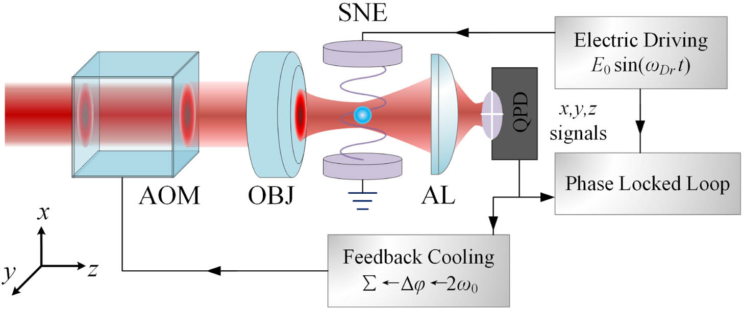
    Fig. 1. Schematic of the experimental setup. The setup consisted of a single-beam optical trap, triaxial position detection and parametric feedback scheme, electric driving, and field measurement circuit. OBJ, NA microscope objective; SNE, horizontally placed steel needles; AOM, acousto-optic modulator; AL, aspheric lens; QPD, self-developed quadrant photodetector. Here shows the top view of the setup, and the x,y,z axes represent the horizontal direction, the vertical direction, and the beam propagation direction, respectively.
    Measured electric intensity at the symmetrical midpoint of the electrodes. A nanoparticle with a diameter of 142.8(33) nm and charge of N=4 was captured by the optical trap, and the measurement was carried out at pressure of 10 mbar. Colors blue, red, and yellow represent the electric field components E˜x, E˜y, and E˜z in three axes, respectively, for driving voltage of 1 V. For each component, 21 driving frequencies with intervals of 1 kHz were applied, while each driving frequency was measured 100 times. The final measurement result is shown as an average of the 21 frequency points. The illustration shows the power spectral density of displacement signals in three axes, with the resonant frequencies of 150.2 kHz, 172.5 kHz, and 46.1 kHz, respectively.
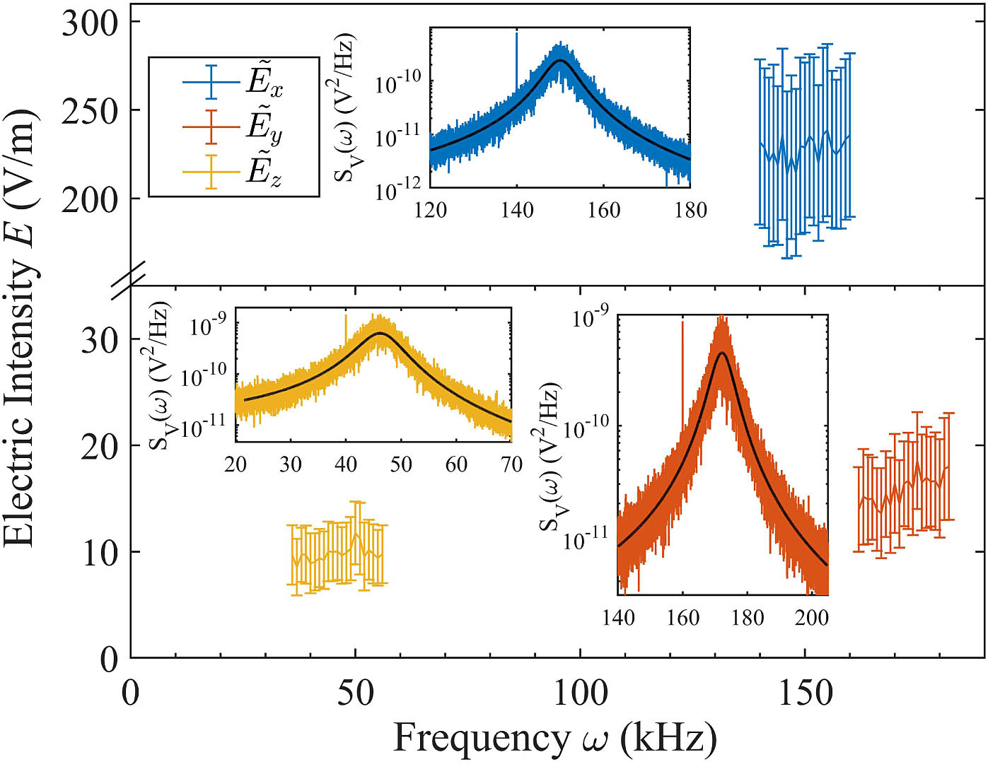
    Fig. 2. Measured electric intensity at the symmetrical midpoint of the electrodes. A nanoparticle with a diameter of 142.8(33) nm and charge of N=4 was captured by the optical trap, and the measurement was carried out at pressure of 10 mbar. Colors blue, red, and yellow represent the electric field components E˜x, E˜y, and E˜z in three axes, respectively, for driving voltage of 1 V. For each component, 21 driving frequencies with intervals of 1 kHz were applied, while each driving frequency was measured 100 times. The final measurement result is shown as an average of the 21 frequency points. The illustration shows the power spectral density of displacement signals in three axes, with the resonant frequencies of 150.2 kHz, 172.5 kHz, and 46.1 kHz, respectively.
    (a) x component of electric intensity along the x,y,z coordinate axes. To intuitively show the variation trend, the normalized value of Ex at each point is normalized by setting the x component E0 at the center point to 1. (b) Vector field plot of (Ex,Ez) in the x–z plane. The grid spacings in the x-axis and z-axis directions are 60 μm and 100 μm, respectively. The notation above indicates the scale of the arrow.
    Fig. 3. (a) x component of electric intensity along the x,y,z coordinate axes. To intuitively show the variation trend, the normalized value of Ex at each point is normalized by setting the x component E0 at the center point to 1. (b) Vector field plot of (Ex,Ez) in the xz plane. The grid spacings in the x-axis and z-axis directions are 60 μm and 100 μm, respectively. The notation above indicates the scale of the arrow.
    (a) Displacement spectral densities for nano-resonators in high vacuum. Gray dashed line, detection noise; light dashed line, fit to the thermomechanical noise model; dark solid line, superposition of thermomechanical noise and detection noise, that is, theoretical transfer function of nano-resonator. At 10−4 mbar, the cooling temperature and damping of the x axis resonant frequency were 500(6) mK and 190.4(54) Hz, respectively. The cross talk from the other two axes brought four additional modes, as annotated in the figure. At higher vacuum, the nano-resonator was cooled to 5.1(4) mK with damping of 55.1(78) Hz. The eigenmode was increased by about 22 kHz due to the larger trapping power, making the cross talk modes further away and not visible in the original frequency band; meanwhile, the parameter feedback signal of the z axis appeared instead. (b) Noise equivalent force (NEF) and equivalent electric intensity (NEEF). The charges of the nano-resonator are set to 100e. Indicated frequency bands represent the range over which the NEF is within 3 dB above the thermodynamic limit (dashed lines).
    Fig. 4. (a) Displacement spectral densities for nano-resonators in high vacuum. Gray dashed line, detection noise; light dashed line, fit to the thermomechanical noise model; dark solid line, superposition of thermomechanical noise and detection noise, that is, theoretical transfer function of nano-resonator. At 104  mbar, the cooling temperature and damping of the x axis resonant frequency were 500(6) mK and 190.4(54) Hz, respectively. The cross talk from the other two axes brought four additional modes, as annotated in the figure. At higher vacuum, the nano-resonator was cooled to 5.1(4) mK with damping of 55.1(78) Hz. The eigenmode was increased by about 22 kHz due to the larger trapping power, making the cross talk modes further away and not visible in the original frequency band; meanwhile, the parameter feedback signal of the z axis appeared instead. (b) Noise equivalent force (NEF) and equivalent electric intensity (NEEF). The charges of the nano-resonator are set to 100e. Indicated frequency bands represent the range over which the NEF is within 3 dB above the thermodynamic limit (dashed lines).
    (a) Linearity and linear range measurement of the nano-resonator. The x axis component of the electric field generated by the AC driving voltage was used for testing. The measurement duration of each data point is 1 s. A goodness of 0.9999 was obtained by fitting the measured results with Efit=αUdr and α=227.1 m−1. Linearity was characterized by the deviation between the measured results and the fitting values, which was calculated by (Ex −Efit)/Efit×100%. The measurements for Udr >0.5V and Udr ≤0.5V were carried out at 3.7×10⁻² mbar and 5×10⁻⁵ mbar, respectively. Here δE is the standard deviation of Ex. (b) Detector signal versus particle displacement. Simulation is based on the model in Ref. [39] with a laser power of 100 mW, beam waist of 662 nm for NA=0.8 objective, particle diameter of 145 nm, collection lens with NA=0.55 and f=1.2 cm, and power received by each photodiode of 5 mW. The blue dashed line represents the linear fitting around the center region of the curve, which is attained by the least squares method, and the R-square is 0.9999. The red line represents the nonlinearity (relative error) between the curve and its linear fitting.
    Fig. 5. (a) Linearity and linear range measurement of the nano-resonator. The x axis component of the electric field generated by the AC driving voltage was used for testing. The measurement duration of each data point is 1 s. A goodness of 0.9999 was obtained by fitting the measured results with Efit=αUdr and α=227.1  m1. Linearity was characterized by the deviation between the measured results and the fitting values, which was calculated by (ExEfit)/Efit×100%. The measurements for Udr>0.5V and Udr0.5V were carried out at 3.7×10²  mbar and 5×10⁵  mbar, respectively. Here δE is the standard deviation of Ex. (b) Detector signal versus particle displacement. Simulation is based on the model in Ref. [39] with a laser power of 100 mW, beam waist of 662 nm for NA=0.8 objective, particle diameter of 145 nm, collection lens with NA=0.55 and f=1.2  cm, and power received by each photodiode of 5 mW. The blue dashed line represents the linear fitting around the center region of the curve, which is attained by the least squares method, and the R-square is 0.9999. The red line represents the nonlinearity (relative error) between the curve and its linear fitting.
    Using optically levitated nanoparticle as nano-resonator to measure the electric field intensity near beam focus.
    Fig. 6. Using optically levitated nanoparticle as nano-resonator to measure the electric field intensity near beam focus.
    PSD of motion signal along the x axis at 10 mbar. The charges on nanoparticle were 4e, and a driving signal with voltage amplitude of Udr=5 V and frequency of ωdr=140 kHz was applied on the electrodes. The motion signal with a duration of τ=2.72 s was obtained at a sampling rate of 1.88 MHz. The resonance frequency ωx=150.2 kHz and damping rate Γx=8544(302) Hz were obtained by Lorentz fitting.
    Fig. 7. PSD of motion signal along the x axis at 10 mbar. The charges on nanoparticle were 4e, and a driving signal with voltage amplitude of Udr=5  V and frequency of ωdr=140  kHz was applied on the electrodes. The motion signal with a duration of τ=2.72s was obtained at a sampling rate of 1.88 MHz. The resonance frequency ωx=150.2  kHz and damping rate Γx=8544(302)  Hz were obtained by Lorentz fitting.
    Partial display of TEM result of particles from Nanocym. The measured diameter of each particle is indicated in the figure, and the mean value and deviation is 142.8(33) nm.
    Fig. 8. Partial display of TEM result of particles from Nanocym. The measured diameter of each particle is indicated in the figure, and the mean value and deviation is 142.8(33) nm.
    Pseudo-color maps of the potential applied to the electrodes and the intensity of the generated electric field. (a), (b) and (c), (d) correspond to the simulation results in the horizontal section (x–z plane) and vertical section (y–z plane), respectively. (a) and (c) show the potential distribution, while (b) and (d) show the distribution of generated electric field. The results in (b) correspond to the area of red solid border that centers around the electrodes in (a). The results in black dashed border in (b) indicate the field range detected by the nano-resonator in experiment. (c) corresponds to the section of the red dashed line in (a).
    Fig. 9. Pseudo-color maps of the potential applied to the electrodes and the intensity of the generated electric field. (a), (b) and (c), (d) correspond to the simulation results in the horizontal section (xz plane) and vertical section (yz plane), respectively. (a) and (c) show the potential distribution, while (b) and (d) show the distribution of generated electric field. The results in (b) correspond to the area of red solid border that centers around the electrodes in (a). The results in black dashed border in (b) indicate the field range detected by the nano-resonator in experiment. (c) corresponds to the section of the red dashed line in (a).
    Noise equivalent displacement and electric intensity for varying optical shot noise level. (a) Noise equivalent displacement combining thermomechanical noise and optical shot noise at three different shot noise levels. ωx=2π×150 kHz, Γcool=16 Hz, m=3×10⁻¹⁸ kg, Tcool=2 mK. (b) Noise equivalent electric intensity based on the displacement noise in (a). N=100.
    Fig. 10. Noise equivalent displacement and electric intensity for varying optical shot noise level. (a) Noise equivalent displacement combining thermomechanical noise and optical shot noise at three different shot noise levels. ωx=2π×150  kHz, Γcool=16  Hz, m=3×10¹⁸  kg, Tcool=2  mK. (b) Noise equivalent electric intensity based on the displacement noise in (a). N=100.
    Controlling the net charge on nanoparticle. Top, to obtain the voltage step of a single charge by multiple short discharge processes. At 1 mbar, a drive signal with an amplitude of Udr1=25 V was applied to the electrodes, and the duration of each discharge process was about 1 s. The charge of nanoparticle varied with discrete steps in the range of 4qe−7qe. A single charge step of δU=583.7(29) μV was calculated by averaging the voltage difference value between two adjacent steps. Bottom, to drastically increase the charge on nanoparticle by a long discharge process. The initial charge of nanoparticle was 6qe and then adjusted to a higher value after a 5 s discharge process. Because the nanoparticle with high net charge entered the nonlinear region of the trap with driving signal of Udr1=25 V, its charge cannot be calculated directly. The driving signal was first turned off and then applied again with a smaller voltage of Udr2=2.5 V. The voltage step of a single charge changed to δU·Udr2 /Udr1. Using the average voltage amplitude, the corresponding nanoparticle charge was calculated as N=99.0(12).
    Fig. 11. Controlling the net charge on nanoparticle. Top, to obtain the voltage step of a single charge by multiple short discharge processes. At 1 mbar, a drive signal with an amplitude of Udr1=25  V was applied to the electrodes, and the duration of each discharge process was about 1 s. The charge of nanoparticle varied with discrete steps in the range of 4qe7qe. A single charge step of δU=583.7(29)  μV was calculated by averaging the voltage difference value between two adjacent steps. Bottom, to drastically increase the charge on nanoparticle by a long discharge process. The initial charge of nanoparticle was 6qe and then adjusted to a higher value after a 5 s discharge process. Because the nanoparticle with high net charge entered the nonlinear region of the trap with driving signal of Udr1=25  V, its charge cannot be calculated directly. The driving signal was first turned off and then applied again with a smaller voltage of Udr2=2.5  V. The voltage step of a single charge changed to δU·Udr2/Udr1. Using the average voltage amplitude, the corresponding nanoparticle charge was calculated as N=99.0(12).
    Shaocong Zhu, Zhenhai Fu, Xiaowen Gao, Cuihong Li, Zhiming Chen, Yingying Wang, Xingfan Chen, Huizhu Hu. Nanoscale electric field sensing using a levitated nano-resonator with net charge[J]. Photonics Research, 2023, 11(2): 279
    Download Citation