Shaocong Zhu, Zhenhai Fu, Xiaowen Gao, Cuihong Li, Zhiming Chen, Yingying Wang, Xingfan Chen, Huizhu Hu, "Nanoscale electric field sensing using a levitated nano-resonator with net charge," Photonics Res. 11, 279 (2023)
Copy Citation Text
The nanomechanical resonator based on a levitated particle exhibits unique advantages in the development of ultrasensitive electric field detectors. We demonstrate a three-dimensional, high-sensitivity electric field measurement technology using the optically levitated nanoparticle with known net charge. By scanning the relative position between nanoparticle and parallel electrodes, the three-dimensional electric field distribution with microscale resolution is obtained. The measured noise equivalent electric intensity with charges of reaches the order of μ at . Linearity analysis near resonance frequency shows a measured linear range over 91 dB limited only by the maximum output voltage of the driving equipment. This work may provide an avenue for developing a high-sensitivity electric field sensor based on an optically levitated nano-resonator.
1. INTRODUCTION
The ability to characterize static and time-dependent electric fields in situ with high sensitivity and high spatial resolution has profound applications for both fundamental science and technology. Precision sensing of electric fields and forces that couple to charge is the most direct way to search for deviations from Coulomb’s law, which may be motivated by the presence of new forces under which dark matter could be charged [1,2]. Recent theoretical models point out that such new forces can weakly mix with electromagnetism, resulting in new Coulomb-like interactions [3]. Traditional electric field sensors to date mainly include dipole antenna-coupled electronics [4], electro-optic crystals [5–7], and resonant MEMS structures [8–10]. In addition, recently emerging Rydberg atom-based sensors have demonstrated the capabilities of electric field distribution measurement with submillimeter spatial resolution [11,12] and the highest sensitivity up to the order of μ ever reported from radio frequency to microwave electric fields [13–15]. More recently, using quantum-entangled trapped ions, measurement of electric fields has reached a sensitivity of at [16], which is several orders of magnitude better than the classical counterpart [17–19].
The levitated nanomechanical resonator exhibits unique advantages in the development of precise force [20–22] and acceleration sensors [23,24] at the micro- and nanoscale, attributed to its high-sensitivity and potential for miniaturization [25]. The nanomechanical system optically levitates the charged dielectric nanoparticle in high vacuum, thus making it a harmonic oscillator sensitive to the surrounding electric field. In case of a weak electric field, the harmonically driven response of the oscillator’s displacement is directly proportional to the electric intensity at its location and the net charge it carries. Therefore, on the premise of knowing the net charge, ultra-high force detection sensitivity means ultra-high electric field detection sensitivity.
In the present study, we extend previous works on highly sensitive force detection using an optically levitated nano-resonator [26] to a novel, three-dimensional, high-sensitivity electric field measurement technology. Using the parallel plate electrodes as the source of the electric field with known frequency, motion signals of the nanoparticle in the three orthogonal directions are used to measure the electric field vectors of the corresponding axis. By changing the relative positions of the nanoparticle and the electrodes, the electric field of the electrodes is scanned point-by-point, and the three-dimensional electric field mapping ability of the scheme is demonstrated. By applying parametric feedback at (), the force and electric intensity detection sensitivity equivalent from the measured displacement spectral density reach the orders of and μ, respectively. In addition, we demonstrate the measurement of a near-resonance frequency electric signal with a linear range of more than 91 dB. This work may provide an avenue for developing optically levitated nano-resonators into high-precision, continuous broadband electric field sensors.
2. EXPERIMENTAL SETUP
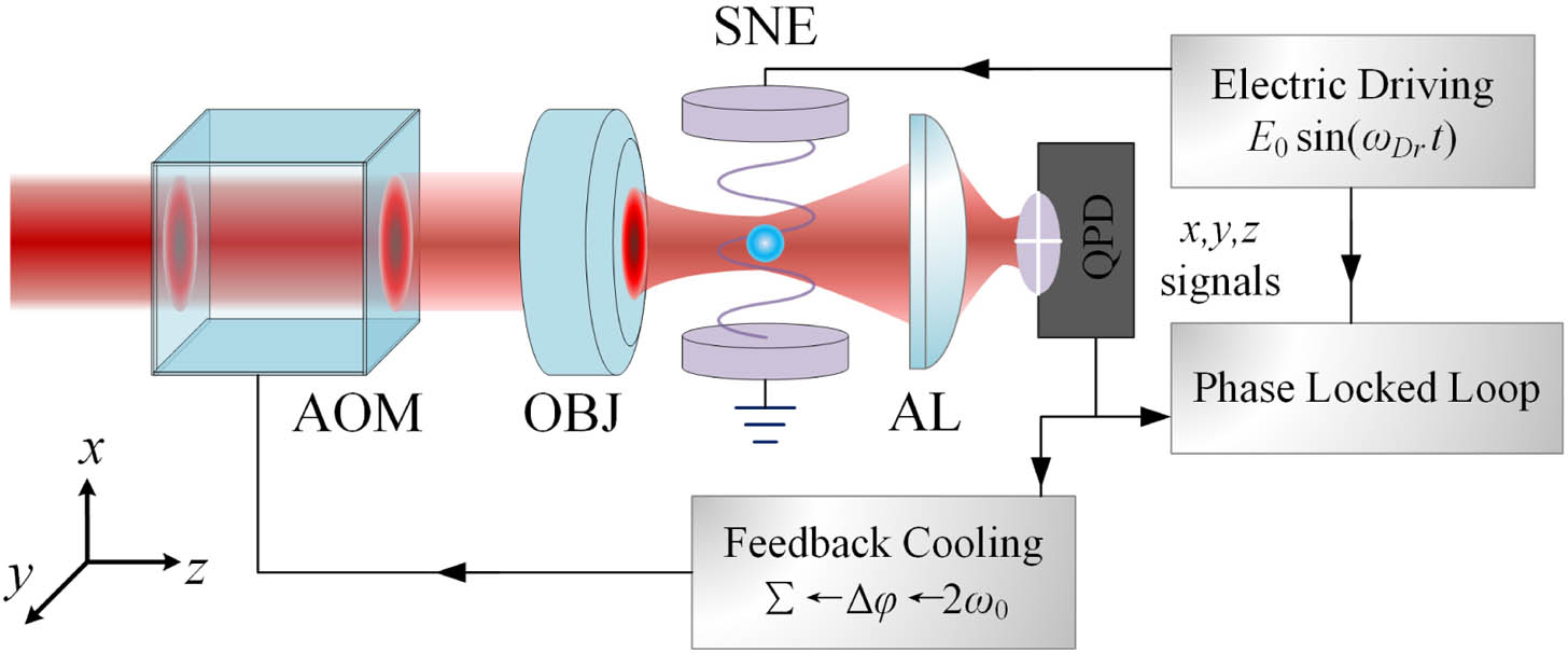
As shown in Fig. 1, the predetermined electric field is generated by applying sinusoidal voltage onto the simplest parallel plate electrodes, and the optically levitated nanoparticle placed within the electric field produces a displacement response to the field. Though this experimental apparatus of the present study is similar to that in Refs. [26,27], it differs in that its electrodes are composed of two horizontal steel (40CrMoV5) needles that are 1 mm in diameter and placed 2.52 mm apart. This allows for producing more distinguishing changes in electric field distribution around the light field. Similar to most previously published studies, the electrodes in Refs. [28,29] are used to calibrate the nanomechanical parameters such as particle mass and the conversion factor from detection voltage to displacement, where the FDTD numerically simulated value of the electric intensity is employed as a known constant. In this study, however, electric intensity generated by the electrodes is no longer a presumed parameter, but a parameter to be detected. To obtain triaxial electric intensity components at each point, an independent triaxial position detection scheme is built to obtain the motion signal along each axis. The electric driving signal is then loaded onto the electrodes, while being synchronously input into the phase locked loops (PLLs) as a reference signal. The PLL extracts the signal components with the same frequency from the input motion signals of three axes. For stable levitation and suppression of frequency fluctuation in high vacuum, a triaxial parametric feedback scheme sums up all the feedback signals and drives a single acousto-optic modulator to cool the center of mass motion of nanoparticles.
Figure 1.Schematic of the experimental setup. The setup consisted of a single-beam optical trap, triaxial position detection and parametric feedback scheme, electric driving, and field measurement circuit. OBJ, NA microscope objective; SNE, horizontally placed steel needles; AOM, acousto-optic modulator; AL, aspheric lens; QPD, self-developed quadrant photodetector. Here shows the top view of the setup, and the axes represent the horizontal direction, the vertical direction, and the beam propagation direction, respectively.
A. Three-Dimensional Electric Field Vector Detection
The electric intensity can be deduced from the driven displacement response and the parameter of the nano-resonator. The relationship between electric field component and displacement response of the corresponding axis (taking the axis for example) is as follows: Here is the mass of the nanoparticle, is the driving frequency of the electric field to be detected, and and are the resonant frequency and damping rate of the nano-resonator, respectively. is the net charge number of the nanoparticle, and is the elementary charge. The power spectral density value at the driving frequency can be extracted as the displacement response of the nano-resonator. See Appendix A for the derivation of the above formula.
We first moved the electrodes with a nano-positioning stage to place the particle at the symmetrical midpoint of the electrodes and measured the electric intensity at that point. As shown in Fig. 2, the normalized measured value of three orthogonal components are , , and , respectively, corresponding to the case where the voltage amplitude applied at the electrodes is 1 V. The electrodes are basically capacitive, and the measured equivalent impedance is about 3 pF, which means that the response electric field within 1 MHz is almost frequency independent. According to the simulation result of COMSOL, three electric intensity components at this point are , , and , respectively, which deviate slightly from the measured values. The discrepancy between the measured and theoretical values may be a result of manufacturing error and alignment error of two steel needles, as well as the relative position error between the symmetrical midpoint and the nanoparticle.
Figure 2.Measured electric intensity at the symmetrical midpoint of the electrodes. A nanoparticle with a diameter of 142.8(33) nm and charge of was captured by the optical trap, and the measurement was carried out at pressure of 10 mbar. Colors blue, red, and yellow represent the electric field components , , and in three axes, respectively, for driving voltage of 1 V. For each component, 21 driving frequencies with intervals of 1 kHz were applied, while each driving frequency was measured 100 times. The final measurement result is shown as an average of the 21 frequency points. The illustration shows the power spectral density of displacement signals in three axes, with the resonant frequencies of 150.2 kHz, 172.5 kHz, and 46.1 kHz, respectively.
Taking the above position as the center point, we moved the relative positions of the nanoparticle and the electrodes along three orthogonal axes and obtained the component of electric intensity at each point, as shown in Fig. 3(a). The variation trend of along each axis is consistent with the theoretical simulation results. In addition, the other two components can also be measured by using the motion signals of the other two axes in the same way and comparing them with the simulation results.
Figure 3.(a) component of electric intensity along the coordinate axes. To intuitively show the variation trend, the normalized value of at each point is normalized by setting the component at the center point to 1. (b) Vector field plot of in the plane. The grid spacings in the -axis and -axis directions are 60 μm and 100 μm, respectively. The notation above indicates the scale of the arrow.
There may be two causes for the deviations of the theory to the measurements near the edges of the vertical and horizonal positions. First, there is a deviation between the simulation and the actual situation. The simple simulation is based on the case that the relative position of the electric field and the center of the optical trap is fixed. However, the relative position of the moving electrodes with the objective and lens changes in experiment, and the measured electric field may be affected slightly by the zero potential of these metal devices.
Second, the initial position error of the nanoparticle in the electric field may be another cause. The nanoparticle should be placed initially in the symmetric center of the electrodes. In the plane, we adjusted the position of the particle as close to the symmetric center of the electrodes as possible by the CCD imaging above the chamber. However, in the plane, the imaging method could not work for alignment, so we measured at different positions by changing the electrode position along the axis. Based on the trend of simulated in the axis as shown in Fig. 3(a), the position with the largest measured was regarded as the middle position in the axis. However, when there was alignment error (either translation error or rotation error) between electrodes, the method would cause certain error to the initial position.
Three-dimensional electric field mapping was realized by obtaining the resultant vectors of each component at different array points. Taking the case of the plane (section ), the resultant vectors of and components in this plane were measured, as shown in Fig. 3(b), together with the results of COMSOL simulation. The parameters of the simulation model and the simulation process are detailed in Appendix B.
C. Noise Equivalent Electric Intensity
The electric intensity detection sensitivity of the nano-resonator depends on its force detection sensitivity, which can be improved by restraining thermal noise in high vacuum. But the accompanying frequency fluctuation in high vacuum would increase the complexity of model fits from the thermal noise response and the electric driven response near the resonance frequency [30]. Both issues can result in significant inaccuracies in the conversion from displacement to electric intensity with a calibrated transfer function. By applying feedback cooling, the nano-resonator can be levitated stably in high vacuum, and the frequency drift effect caused by the non-linearity of the optical trap can be suppressed, which makes the nano-resonator more stable in response to near-resonance driving forces. Therefore, feedback cooling is indispensable for realizing ultrasensitive electric field detection, although theoretically it does not improve the detection sensitivity at certain pressure conditions (see Appendix C). The displacement noise floors of nano-resonators were measured at different pressures, where the electrodes and other metal structures in the chamber were grounded to isolate the residual electric field. The resulting displacement spectral densities in high vacuum for two nano-resonators with parametric feedback cooling are shown in Fig. 4(a). The fits of the displacement spectral density to the expected thermomechanical noise response superimposed on the detection noise for the nano-resonator with different feedback damping show close agreement. Beside the axis resonant frequency, the additional modes originating from cross talk of other axes are generally visible in the thermomechanical noise response.
Figure 4.(a) Displacement spectral densities for nano-resonators in high vacuum. Gray dashed line, detection noise; light dashed line, fit to the thermomechanical noise model; dark solid line, superposition of thermomechanical noise and detection noise, that is, theoretical transfer function of nano-resonator. At , the cooling temperature and damping of the axis resonant frequency were 500(6) mK and 190.4(54) Hz, respectively. The cross talk from the other two axes brought four additional modes, as annotated in the figure. At higher vacuum, the nano-resonator was cooled to 5.1(4) mK with damping of 55.1(78) Hz. The eigenmode was increased by about 22 kHz due to the larger trapping power, making the cross talk modes further away and not visible in the original frequency band; meanwhile, the parameter feedback signal of the axis appeared instead. (b) Noise equivalent force (NEF) and equivalent electric intensity (NEEF). The charges of the nano-resonator are set to . Indicated frequency bands represent the range over which the NEF is within 3 dB above the thermodynamic limit (dashed lines).
The thermal noise dominates over frequency range near resonance while the noise floor closely approaches the optical shot noise limit over that far from resonance. Comparing the displacement spectral density at and , a reduction in gas damping, due to the balance between the thermomechanical noise and shot noise, the frequency range over which the spectral density is thermal noise limited, is clearly narrowed. The theoretical force transfer function of the nano-resonator can be calculated based on the resonant frequency and damping as follows:
The displacement spectral densities in Fig. 4(a) are converted to a noise equivalent force (NEF) by dividing the displacement spectral densities by the amplitude of theoretical transfer function above, as shown in the right side of Fig. 4(b). Further, the noise equivalent electric intensity (NEEF) can be obtained by dividing the NEF by the charges as shown in the left side.
As expected, the NEF and NEEF both reach the thermal noise limit near resonance frequency. When the damping is lower in higher vacuum, a lower thermodynamic limit could be provided, meanwhile, which is more difficult to reach since the thermomechanical noise must be above the shot noise. The minimum NEEF reaches the order of μ at , corresponding to the case of , which is lower than that at by more than 1 order of magnitude, and can be further reduced by increasing the net charge or the vacuum level. The bandwidth over which the NEEF is within 3 dB above the thermodynamic limit is 48.6 kHz and 1.1 kHz for two pressures, respectively. This could be further broadened by 1 order of magnitude by adopting a heterodyne detection scheme and optimizing the detection noise to approach the standard quantum limit [31].
As a comparison, the achieved minimum detectable field is superior to the reported performance using Rb Rydberg atoms by 1 order of magnitude [13], approaching the equivalent performance for an antenna dipole electronic sensor with length of 1 cm [14]. One benefit of optically levitated nano-resonators is that the bandwidth of interest within which the thermal noise is above or equal to the shot noise is tunable, and the tunable bandwidth can reach the order of tens of kHz or even hundreds of kHz by tuning the power of trapping beam. For example, realistically one could trap with as little as 50 mW and up to 1 W of laser power, and the corresponding resonant frequency could change from about 100 kHz to about 400 kHz. In contrast, traditional passive dipole electronics usually need to change the structure size to achieve similar effects.
D. Linearity and Linear Range Analysis
As a test of sensing performance for linearity and linear range of electric field sensing in axis, the nano-resonator was moved back to the center point and charged with a high value of (see Appendix D). The measurement was performed at and by applying a sinusoidal electric field with frequency of 140 kHz, which is 10 kHz offset from the resonance to reduce the effect of frequency instability on the measurement. We set a specific driving voltage as a reference first (e.g., 5 V) and recorded the corresponding response of the nanoparticle, as a fiducial value for judging whether the charges would change during the experiment. After applying different driving voltages each time, we changed the driving voltage back to the reference voltage and observed whether the response is different from the fiducial value. When changing the pressure, we also applied a similar method that used a monitoring response value to make sure the charges remained constant. At , we applied driving voltages ranging from 1 V to 160 V and for higher electric field sensitivity at , the same operation was conducted except that the range of driving voltages ranged from 5 mV to 500 mV. Finally, the measurement results at different driving voltages were converted to the measured electric intensities by using Eq. (1) and measurement time of 1 s, as shown in Fig. 5(a).
Figure 5.(a) Linearity and linear range measurement of the nano-resonator. The axis component of the electric field generated by the AC driving voltage was used for testing. The measurement duration of each data point is 1 s. A goodness of 0.9999 was obtained by fitting the measured results with and . Linearity was characterized by the deviation between the measured results and the fitting values, which was calculated by . The measurements for and were carried out at and , respectively. Here is the standard deviation of . (b) Detector signal versus particle displacement. Simulation is based on the model in Ref. [39] with a laser power of 100 mW, beam waist of 662 nm for objective, particle diameter of 145 nm, collection lens with and , and power received by each photodiode of 5 mW. The blue dashed line represents the linear fitting around the center region of the curve, which is attained by the least squares method, and the -square is 0.9999. The red line represents the nonlinearity (relative error) between the curve and its linear fitting.
Within the corresponding measured electric intensities ranging from 1.03 V/m to 36.2 kV/m, which span over 4 orders of magnitude (91 dB), the linearity of electric field sensing was within 10%. The minimum detectable electric field is mainly limited by the detection sensitivity of the nano-resonator at . While further reduction in pressure can lead to higher detection sensitivity, the accompanying instability and drift of resonance frequency become more pronounced, resulting in increased uncertainty and deviation of the measured value. The maximum detectable electric field in this measurement was merely limited by the maximum output of the high-voltage amplifier (Aigtek ATA-2031), and its theoretical limit is related to the linear range of optical force and the capture region of trap [32] and is ultimately limited by the response range of the detection scheme to nanoparticle displacement. Figure 5(b) shows the simulated detector signal in terms of balanced power with particle displacement. For the maximum electric intensity measured in experiment, the amplitude of the electric field force acting on the nanoparticle is about 0.57 pN. Combined with the stiffness of the trap, the corresponding maximum amplitude of particle displacement reached about 0.21 μm, which is still within the linear region of the detector with nonlinearity of . The linear range of the detector with 10% nonlinearity would be about 0.38 μm, corresponding to a larger detectable electric field of value 65.5 kV/m. Theoretically, we can further improve the upper range of the detectable electric field by reducing the charges of the particle. For example, if the charge is reduced to , the corresponding maximum electric field may reach 6.5 MV/m. This is an extreme situation where the escape of nanoparticle, air breakdown, and other issues need to be considered.
4. CONCLUSION
We have demonstrated a high-sensitivity electric field measurement technology using optically levitated nano-resonators. By scanning the electric field distribution between parallel electrodes, the three-dimensional electric field mapping capability of the system was demonstrated. Its measuring spatial resolution depends on the motion amplitude of the nanoparticle in the equilibrium position and the manipulation accuracy of the equilibrium position, which can reach the order of nanometers. Broadband measurement at the thermodynamic limit yields a noise equivalent detection resolution of the order of μ in high vacuum, which is competitive to that of previously reported electric field detection schemes. Linearity analysis near resonance shows a linear range of more than 4 orders of magnitude.
Having higher net charges is the key to further improve the detection resolution of nano-resonators. Although this can be achieved simply by using larger particles, for example, the net charge of the micron-sized particle can reach the order of [24], and the resulting force detection sensitivity is worse due to larger mass. Therefore, the size of the particle needs to be optimized according to these two factors to obtain the optimal electric field detection sensitivity. Although this work is based on optical levitation systems, charged particles in other levitation systems are eligible to be developed into highly sensitive electric field sensors. The advantage of the levitated resonator is that its resonant frequency can be adjusted from Hz to MHz according to size of particle and stiffness of the potential well to meet the application requirements of different frequency bands, especially low-frequency submarine communication.
Our method is most similar to electric field sensing with trapped ions that use mechanical oscillators as exquisite quantum tools to measure small displacements due to weak forces and electric fields, albeit with a very different charge to mass ratio. As schemes with optically levitated nanoparticles do not need an additional DC or AC electric field for a stable trap that is generally utilized in ions schemes, it can eliminate the influence of the existing electric field in the device on the electric field measurement as much as possible. Furthermore, the ion trap scheme is generally sensitive to the electric field in a certain direction, such as the direction of the magnetic field used to generate the cyclotron motion, while a single nanoparticle can be used to measure the three-dimensional vector electric field at the same time, which would be an obvious advantage of this method.
APPENDIX A: ELECTRIC FIELD SENSING WITH A HARMONIC OSCILLATOR
A major benefit of the electric field sensor described in this work is that its dynamic response closely follows that of a one-dimensional viscously damped harmonic oscillator, making it possible to convert from measured nano-resonator displacement to an equivalent electric intensity using a low-order model. In this section, we describe the harmonic oscillator model and the conversion between displacement and electric intensity. Much of the analysis in this section follows directly from the work of Ricci et al. [28] but is specifically focused toward optomechanical electric field sensing.
The simplified diagram of electric field sensing with a optically levitated nano-resonator is described in Fig. 6, where the electric field is generated by a pair of electrodes placed in horizontal direction ( axis direction) perpendicular to the optical axis ( axis direction). A driving signal with amplitude of and frequency of is loaded to the electrodes, which generated a sinusoidal electric field near the nanoparticle. The electric field vector contained three components along orthogonal axes, written as . The motion signal along each axis is the driving response to the corresponding electric field component.
Figure 6.Using optically levitated nanoparticle as nano-resonator to measure the electric field intensity near beam focus.
Figure 7.PSD of motion signal along the axis at 10 mbar. The charges on nanoparticle were , and a driving signal with voltage amplitude of and frequency of was applied on the electrodes. The motion signal with a duration of was obtained at a sampling rate of 1.88 MHz. The resonance frequency and damping rate were obtained by Lorentz fitting.
APPENDIX B: ERROR ESTIMATION AND COMSOL SIMULATION OF ELECTRIC INTENSITY
Obviously, reducing the uncertainty of the nanoparticle mass can improve the accuracy of the electric field measurement. It was observed that both the density and radius of nanoparticles may vary when pressure changing (especially near 1 mbar), which was mainly caused by the separation of surface functional groups [33], and this would bring some systematic errors. However, in the electric sensing experiment, we first reduced the pressure to or even lower and then returned to 10 mbar for calibration and measurement. The density and radius of the nanoparticle no longer changed with the pressure after we conducted this operation. Therefore, we believe that the radius results measured by transmission electron microscopy (TEM, also measured in high vacuum environment and with surface functional group desorption) can be used as reliable prior data. By comparing TEM results of nanoparticle samples from different brands, a nanoparticle with a nominal diameter of 150 nm from Nanocym was selected in experiment, which has a relatively high particle size uniformity. As shown in Fig. 8, the mean value and deviation of particles can be obtained by averaging the size of multiple particles measured by the TEM image.
Figure 8.Partial display of TEM result of particles from Nanocym. The measured diameter of each particle is indicated in the figure, and the mean value and deviation is 142.8(33) nm.
Figure 9.Pseudo-color maps of the potential applied to the electrodes and the intensity of the generated electric field. (a), (b) and (c), (d) correspond to the simulation results in the horizontal section ( plane) and vertical section ( plane), respectively. (a) and (c) show the potential distribution, while (b) and (d) show the distribution of generated electric field. The results in (b) correspond to the area of red solid border that centers around the electrodes in (a). The results in black dashed border in (b) indicate the field range detected by the nano-resonator in experiment. (c) corresponds to the section of the red dashed line in (a).
Figure 10.Noise equivalent displacement and electric intensity for varying optical shot noise level. (a) Noise equivalent displacement combining thermomechanical noise and optical shot noise at three different shot noise levels. , , , . (b) Noise equivalent electric intensity based on the displacement noise in (a). .
In experiment, we used an open-loop electromotive positioning stage (Newport AG-LS25), whose travel range is 12 mm with an absolute positioning accuracy of 100 μm. The step displacement is 50 nm, and we moved 1200 steps and 2000 steps, respectively, to obtain 60 μm and 100 μm sampling interval in two directions. Therefore, the cumulative errors for the actual position of nanoparticles were 0.5 μm and 0.83 μm, respectively.
APPENDIX C: NOISE EQUIVALENT DISPLACEMENT AND ELECTRIC INTENSITY
By extending the drive frequency to the broadband, the relationship between the harmonically driven displacement, , and driving electric intensity, , as a function of frequency, , can be determined from Eq. (A1) by subtracting the Langevin force term,
Here, represents the transfer function between the displacement of the nano-resonator and the driving electric field, which is related to the general force transfer function of the nano-resonator via its net charge:
Further, similar to the force detection sensitivity of the nano-resonator, the equivalent electric intensity due to thermal noise is then
Obviously, is only a function of the resonator parameters (, , , and ) and not a function of frequency, meaning that the thermomechanical noise floor in terms of electric intensity is flat.
When parametric feedback cooling is applied to the nano-resonator, the feedback cooling term is added to Eq. (A1), leading to an increase in the resonant frequency and damping rate [35,36], ultimately changing the transfer function of the harmonic oscillator to
The equivalent electric intensity due to thermal noise with feedback cooling is rewritten as
Here, represents a lower equivalent temperature noted as
Interestingly, can be deduced from Eqs. (C5) and (C6), meaning that feedback cooling does not theoretically affect the equivalent electric intensity of the nano-resonator due to thermal noise. However, in addition to thermomechanical noise, optical shot noise is the other fundamental limiting noise source. The power spectral density of the optical shot noise is , where is Planck’s constant, is the optical frequency of the laser, is the average power reaching the photodetector, and is the quantum efficiency of the photodetector. This can be converted to shot noise in terms of displacement using [37]
Here, and are the transimpedance gain and responsivity of the photodetector, while is the calibration factor. The shot noise in terms of electric intensity is
Unlike the equivalent electric intensity in terms of thermal noise, is a function of frequency and gets the minimum value at the eigenfrequency of the resonator. Since the thermomechanical noise and shot noise are uncorrelated, they can be summed to get the total noise equivalent displacement or electric intensity . Although the optical shot noise does not represent real motion of the nano-resonator, it is detection noise that analytically refers to either displacement or electric force. The best-case scenario for a nano-resonator with fixed parameters is for the thermomechanical noise to be higher than the optical shot noise, which can be done by tuning the power of trapping beam. Within the bandwidth of interest, the optical readout will measure the motion of the resonator with minimal contribution from shot noise. This is shown in Fig. 10, where the calculated noise floor is presented for a resonator with parameters similar to those described in the experiments. Three different levels of shot noise are shown. When the shot noise is reduced by 1 order of magnitude, the bandwidth over which the noise equivalent electric intensity is within 3 dB above the thermodynamic limit increases from 370 Hz to 3.6 kHz by nearly 1 order of magnitude.
APPENDIX D: CONTROLLING THE NET CHARGE ON THE NANOPARTICLE
The net charge on the nanoparticle was controlled by corona discharge generated by high-voltage () electrodes placed about 5 cm away from the nanoparticle in the chamber. A plasma of both positive and negative ions was created and adsorbed on the nanoparticle to change the charge [26,29,38]. Although the charges on the nanoparticle vary randomly, the number of charges varies by an integer multiple. Under a certain frequency driving electric field, by observing the response of the nanoparticle and the minimum step of response change, which corresponds to a single charge, we can determine the charges by dividing the driving response with the minimum step. Figure 11 shows the amplitude and phase that LIA demodulated from the motion signal in axis. The motion signal was a response to the drive signal with frequency of . At 1 mbar, the minimum voltage step was first obtained through multiple short discharge processes, and it can be considered as the voltage change corresponding to a single charge. At this pressure, the net charge of the nanoparticle after multiple discharges was usually less than 10. It is observed that the net charge on nanoparticle could be raised drastically to a higher value by a long discharge process when the pressure was reduced to a range of 0.1–0.5 mbar. In addition, the driving voltage applied during the discharge process also affected the net charge on the nanoparticles. It seems that a higher driving voltage led to a larger net charge as more plasma produced by ambient gas can pass through the nanoparticle. However, nanoparticle tended to enter the nonlinear region of the trap after acquiring high net charge. Therefore, when a large response signal was observed in experiment, the driving voltage should be turned off immediately to prevent the nanoparticle escaping from the trap. At a pressure lower than 0.1 mbar with lower gas molecular density in the chamber, the free path of electrons or ions is longer, and the breakdown voltage required for discharge process is much higher. In this case, ultraviolet lamp irradiation is recommended to control the charges of the nanoparticle.
Figure 11.Controlling the net charge on nanoparticle. Top, to obtain the voltage step of a single charge by multiple short discharge processes. At 1 mbar, a drive signal with an amplitude of was applied to the electrodes, and the duration of each discharge process was about 1 s. The charge of nanoparticle varied with discrete steps in the range of . A single charge step of μ was calculated by averaging the voltage difference value between two adjacent steps. Bottom, to drastically increase the charge on nanoparticle by a long discharge process. The initial charge of nanoparticle was and then adjusted to a higher value after a 5 s discharge process. Because the nanoparticle with high net charge entered the nonlinear region of the trap with driving signal of , its charge cannot be calculated directly. The driving signal was first turned off and then applied again with a smaller voltage of . The voltage step of a single charge changed to . Using the average voltage amplitude, the corresponding nanoparticle charge was calculated as .
[26] Z. Fu, S. Zhu, Y. Dong, X. Chen, X. Gao, H. Hu. Force detection sensitivity spectrum calibration of levitated nanomechanical sensor using harmonic coulomb force. Opt. Laser Eng., 152, 106957(2022).
[27] T. Liang, S. Zhu, P. He, Z. Chen, Y. Wang, C. Li, Z. Fu, X. Gao, X. Chen, N. Li, Q. Zhu. Yoctonewton force detection based on optically levitated oscillator. Fundam. Res..