
Hafiz Saad Khaliq, Inki Kim, Aima Zahid, Joohoon Kim, Taejun Lee, Trevon Badloe, Yeseul Kim, Muhammad Zubair, Kashif Riaz, Muhammad Qasim Mehmood, Junsuk Rho. Giant chiro-optical responses in multipolar-resonances-based single-layer dielectric metasurfaces[J]. Photonics Research, 2021, 9(9): 1667
- Photonics Research
- Vol. 9, Issue 9, 1667 (2021)
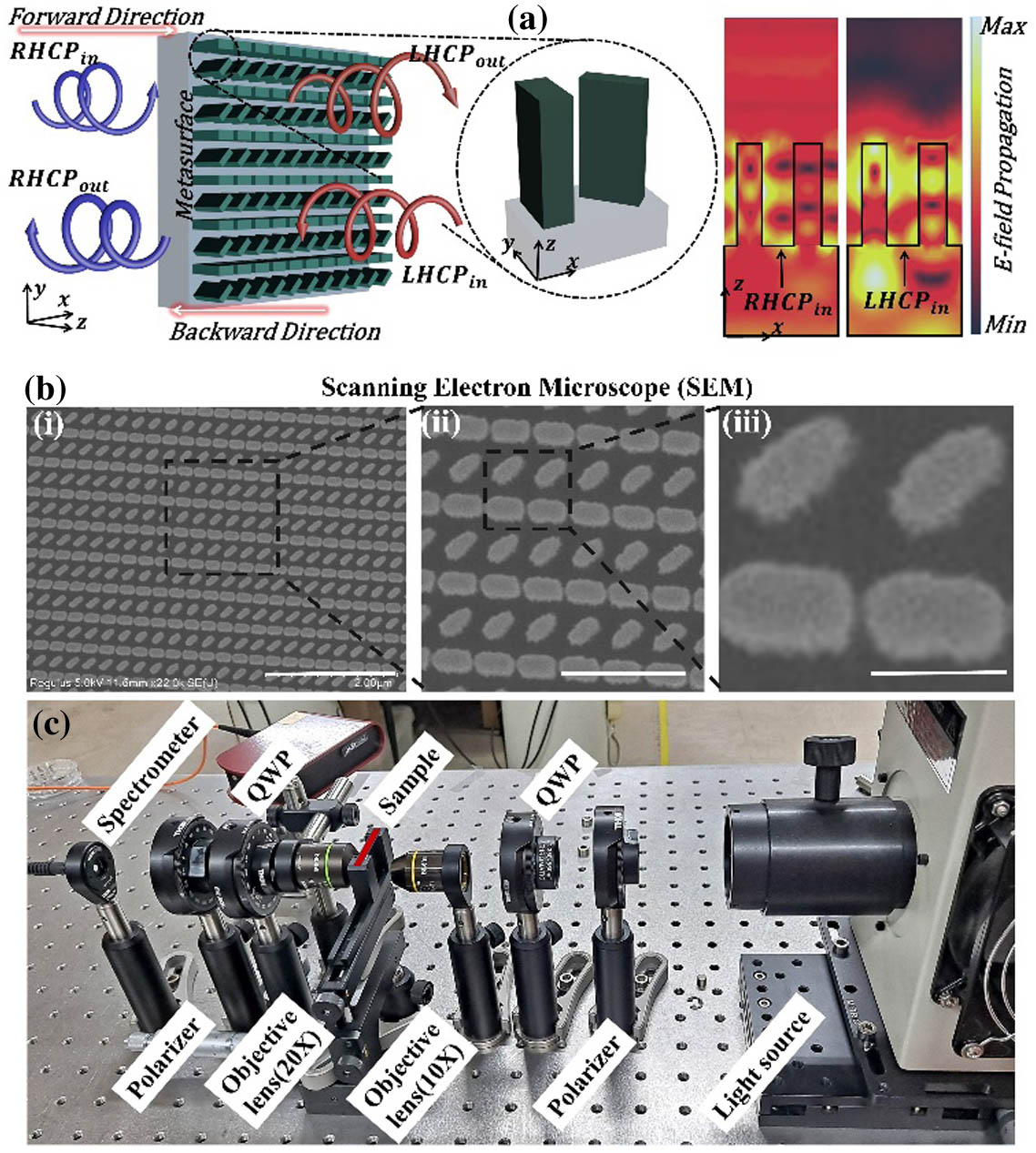
Fig. 1. Working principle of the single-layered all-dielectric diatomic metasurface and optical setup. (a) Schematic image of the working principle of the proposed diatomic metasurface introducing a giant chiro-optical effect in the visible regime. (b) SEM image of a portion of the fabricated diatomic metasurface. The scale bar is (i) 2 μm; (ii) 0.75 μm; (iii) 0.25 μm. (c) The characterization setup of the designed dielectric metasurface for giant chiro-optical effect. An arc lamp housing is used as the light source. A linear polarizer is used to linearly polarize the input beam, passing through a QWP to produce LHCP or RHCP light. The OL focuses on the polarized light, which illuminates the sample. The transmitted light beam from the sample further passes through another OL, QWP, and polarizer. Finally, the results are recorded by using a spectrometer.
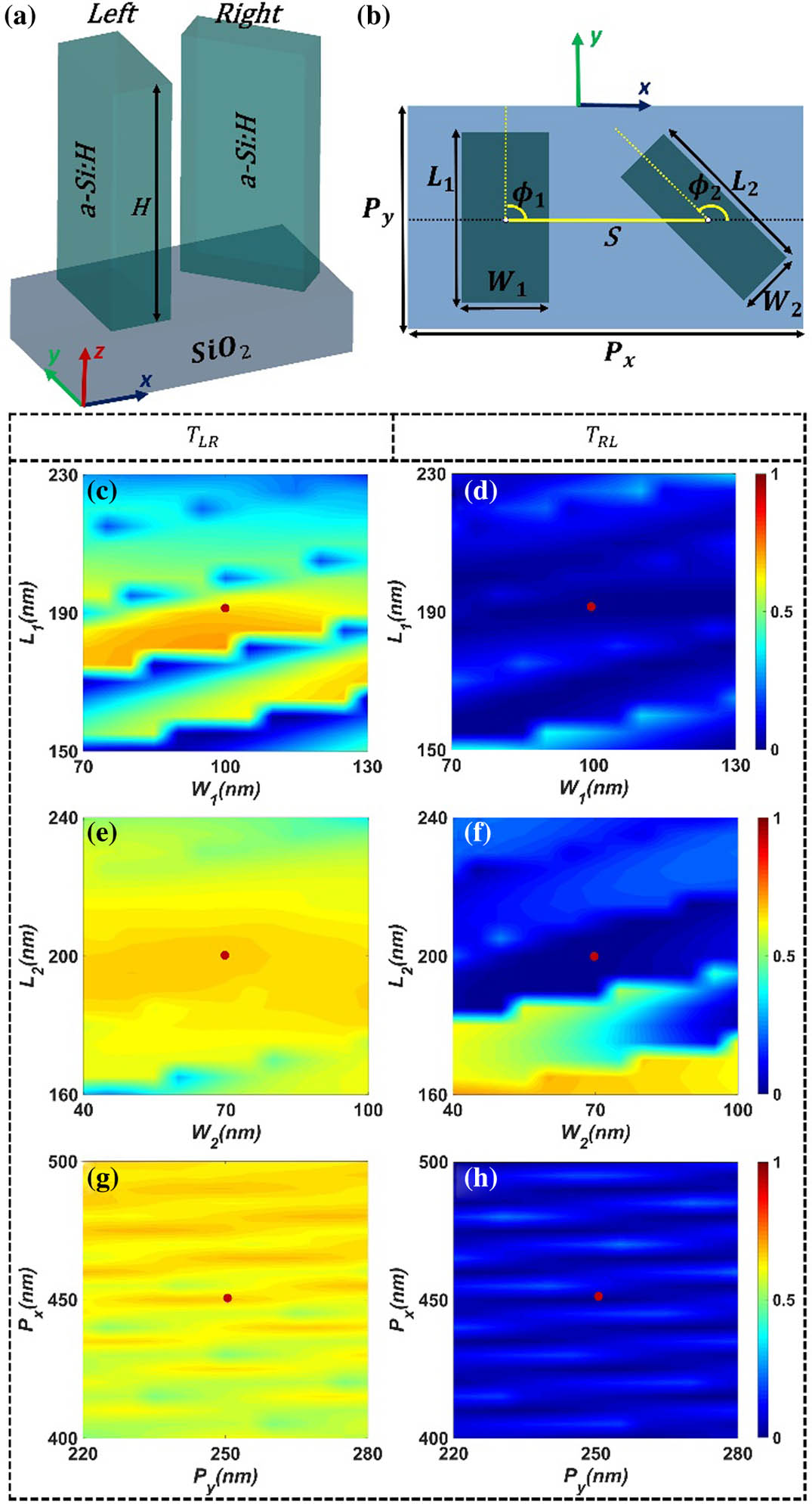
Fig. 2. Optimization of the building block of the diatomic metasurface. (a) 3D perspective view of the building block of the metasurface containing a pair of distinct a-Si:H-based nanofins with a relative angle (Δ ϕ width 1 W 1 = 100 nm length 1 L 1 = 195 nm width 2 W 2 = 70 nm length 2 L 2 = 200 nm S = 227.5 nm x P x = 455 nm y P y = 255 nm H = 400 nm S , P x , P y H L 1 × W 1 L 2 × W 2 x y
Fig. 3. Representation of parameters of the Jones matrix for designed metasurface in transmission and reflection. The simulated coefficients of the Jones matrix in transmission (T LR T RL T RR T LL
Fig. 4. AT parameter dependence on the incident angle of light. AT parameter in the forward direction for a wide range of incident angles in (a) x z y z
Fig. 5. Scattering power in terms of multipolar resonances. Calculated normalized multipolar decomposition for individual nanofins of the diatomic structure for (a), (b) RHCP and (c), (d) LHCP illumination in the forward direction. The red, blue, green, magenta, and black curves show the scattering power for the ED, MD, TD, EQ, and MQ modes, respectively.
Fig. 6. Electric and magnetic field distributions at different wavelengths in the visible regime. Calculated normalized EM field distributions at different wavelengths in the visible regime for the individual nanofins for RHCP and LHCP incident light. The normalized electric field distributions for the left and right nanofins at the wavelengths of 550, 640, and 700 nm for (a)–(f) RHCP and (g)–(i) LHCP illumination. Similarly, the normalized magnetic field distributions for the left and right nanofins at the wavelengths of 550, 640, and 700 nm for (m)–(r) RHCP and (s)–(x) LHCP illumination. The blue lines with white arrows show the direction of electric currents.
|
Table 1. Comparison of the Relevant Literature of All-Dielectric Structures with the Proposed Design

Set citation alerts for the article
Please enter your email address
© Copyright 2018-2021 | Chinese Laser Press. All Rights Reserved 沪ICP备15018463号-20