Author Affiliations
1Cornell University, Department of Physics, Ithaca, New York, United States2Cornell University, School of Applied and Engineering Physics, Ithaca, New York, United Statesshow less
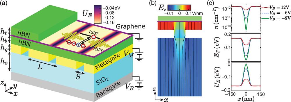
Fig. 1. Engineering of SL electric potential in graphene. (a) Physical realization: field-effect carrier density modulation using a metagate/backgate combination. Inset: SL potential on a schematically exposed graphene plane (). (b) Electrostatic simulation of (a): (color-coded) and the electric field lines in the plane. (c) The doped carrier density (top), the Fermi level (middle), and the SL electric potential (bottom) for three backgate voltages: (dotted red), (dashed blue), and (solid green). Backgate/metagate parameters for (a)–(c): , , , , , , and .
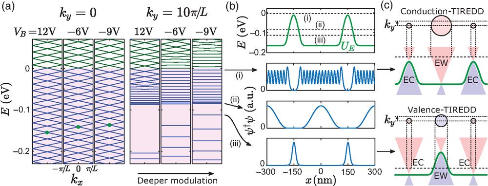
Fig. 2. The TIREDD mechanism is responsible for flat subbands of graphene electrons in SL electric potentials. (a) Left: no intersubband gaps for Dirac electrons due to Klein tunneling. Filled bands ( < ): blue, unoccupied bands > : green. Green dots: original Dirac crossing points prior to band folding. Right: emergence of intersubband gaps for large- electrons, strongly modulated SL potential. (b) Top, dashed lines: energy levels of several examples of bound states located right below the Fermi surface (i) at the lowest energy of the conduction-band TIREDD and (ii) at the highest energy of the valence band TIREDD. The energy levels are defined relative to the SL potential landscape (). Solid green line: SL electric potential . Bottom three: wave function amplitudes of (i)–(iii). Negligible tunneling between the adjacent SL periods: emergence of the flat subbands. (c) TIREDD of (top) conduction and (bottom) valence band Dirac electrons. Circles: iso-energy contours in the momentum space at the centers of the EW and EC regions. Dashed lines: energy levels, green lines: the SL potential. SL parameters: same as in Fig. 1.
Fig. 3. The massless dispersion of Dirac electrons makes the ISBT energy be nearly uniform over a broad region of the Fermi surface (). The electronic subband structure ( case) is shown along at a fixed ; any choice of value would produce similar subband dispersions along , since the subbands at moderately high become flat in direction, as shown in Fig. 2(a). Each vertical black bar is given as a guide to the eye for denoting a vertical transition () from an occupied state below the Fermi surface to a state above the Fermi surface, and all bars have the same length. In this case, the ISBT energy appears as very uniform roughly within , which is almost 45% of the whole area of the Fermi surface .
Fig. 4. Optical conductivity and ISBT resonances for SL-modulated graphene electrons. (a) Real part of the conductivity calculated for . With strongly modulated SL potentials (, ), ISBTs are manifested as Lorenzian peaks in . (b) Both real (left) and imaginary (right) parts of the conductivity calculated at (top) and (bottom); solid thin black: no modulation (), dotted red: , dashed blue: , and solid thick green: .
Fig. 5. HIPP dispersion with USC and far-field detection of HIPPs. (a) Density of states or for visualizing the polaritonic dispersion, calculated with Drude conductivity model that cannot capture the ISBT features. (b) Reflection spectra (light polarized along the axis and normal incidence) at low frequency (below the first plasmonic bandgap) calculated with Drude conductivity model; dotted red: , dashed blue: , and solid green: . (c) Density of states calculated with Kubo conductivity as given in Eq. (3); the white dashed lines in panel are denoting the same frequencies of the ISBT resonances () shown in Fig. 4(a), and the corresponding (d) reflection spectra. (e) The same results as in panel (c) zoomed at a low-frequency and low-momentum window; the star markers refer to the HIPP modes at that appear as resonant peaks in the reflection spectra in (d), and the white dotted lines are guides to the eye for the lowest and the second lowest HIPP bands.