• Advanced Photonics
  • Vol. 5, Issue 2, 026004 (2023)
Minwoo Jung1、* and Gennady Shvets2、*
Author Affiliations
  • 1Cornell University, Department of Physics, Ithaca, New York, United States
  • 2Cornell University, School of Applied and Engineering Physics, Ithaca, New York, United States
  • show less
    DOI: 10.1117/1.AP.5.2.026004 Cite this Article Set citation alerts
    Minwoo Jung, Gennady Shvets. Emergence of tunable intersubband-plasmon-polaritons in graphene superlattices[J]. Advanced Photonics, 2023, 5(2): 026004 Copy Citation Text show less

    Abstract

    On-demand modification of the electronic band structures of high-mobility two-dimensional (2D) materials is of great interest for various applications that require rapid tuning of electrical and optical responses of solid-state devices. Although electrically tunable superlattice (SL) potentials have been proposed for band structure engineering of the Dirac electrons in graphene, the ultimate goal of engineering emergent quasiparticle excitations that can hybridize with light has not been achieved. We show that an extreme modulation of one-dimensional (1D) SL potentials in monolayer graphene produces ladder-like electronic energy levels near the Fermi surface, resulting in optical conductivity dominated by intersubband transitions (ISBTs). A specific and experimentally realizable platform comprising hBN-encapsulated graphene on top of a 1D periodic metagate and a second unpatterned gate is shown to produce strongly modulated electrostatic potentials. We find that Dirac electrons with large momenta perpendicular to the modulation direction are waveguided via total internal reflections off the electrostatic potential, resulting in flat subbands with nearly equispaced energy levels. The predicted ultrastrong coupling of surface plasmons to electrically controlled ISBTs is responsible for emergent polaritonic quasiparticles that can be optically probed. Our study opens an avenue for exploring emergent polaritons in 2D materials with gate-tunable electronic band structures.

    1 Introduction

    Polaritons in two-dimensional (2D) semiconductor materials (e.g., plasmon-polaritons in graphene1,2 or exciton–trion polaritons in transition metal dichalcogenides3,4) have attracted significant interest as a promising platform for developing novel optoelectronic devices because of the variety of tools for controlling the density of carriers. Photocarrier injection via high-intensity pulses is useful to probe ultrafast transient responses of such polaritons,57 and capacitive field-effect gating is exploited for active control over steady-state responses. Although a uniform gate can tune overall polariton dispersions due to carrier density dependence of Drude weight in graphene1,2 and exciton/trion oscillator strengths in transition metal dichalcogenides,8 more exotic electro-optic controls can be achieved using a metagate—a gating structure with spatially varying capacitance. Especially in graphene plasmonics, spatial modulation of carrier densities via metagate tuning has been considered for various applications, such as local phase modulation,9 topological phase switching,10 and Bloch polariton steering.11

    Owing to quantum capacitance effect,12 spatially modulated carrier densities n(r) under electrochemical equilibrium give rise to superlattice (SL) electric potentials UE(r) for Dirac electrons, given as vFπn(r)+UE(r)=μ0,where vF is the Fermi velocity of Dirac electrons (assumed to be density-dependent: vF(n)=[0.85+0.035ln(n0/n)]×106  m/s, where n0=1015  cm213) and μ0 is the constant electrochemical potential (assumed to be μ0=0 for grounded graphene). Therefore, any modulation of the chemical potential EF(x)=vFπn(r) must be matched by the opposite modulation of the SL potential UE(x)=EF(x). Additional effects, such as image charges produced by the metagate,14 may become important with an extremely thin spacer dielectric between graphene and metagate (e.g., in our proposed system, see Fig. 1, Uimage=e216πϵhBNhb100  meV, where ϵhBN=4 and hb=1  nm); however, we choose the spacer thickness to be reasonably thick (hb=10  nm) so that the SL potential modulation depth owing to image charges is negligible (Uimage<9  meV with hb=10  nm).

    Engineering of SL electric potential in graphene. (a) Physical realization: field-effect carrier density modulation using a metagate/backgate combination. Inset: SL potential UE(x) on a schematically exposed graphene plane (VB=−9 V). (b) Electrostatic simulation of (a): Ez (color-coded) and the electric field lines in the x−z plane. (c) The doped carrier density n(x) (top), the Fermi level EF(x) (middle), and the SL electric potential UE(x) (bottom) for three backgate voltages: VB=12 V (dotted red), VB=−6 V (dashed blue), and VB=−9 V (solid green). Backgate/metagate parameters for (a)–(c): ht=5 nm, hb=10 nm, hg=10 nm, h0=150 nm, L=300 nm, S=80 nm, and VM=1 V.

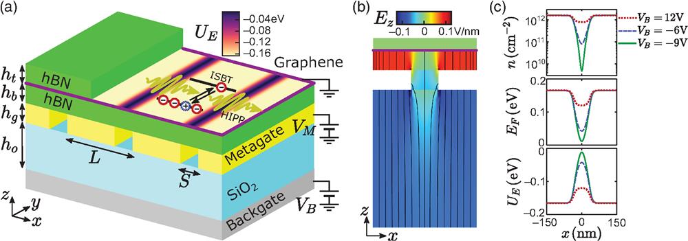
    Figure 1.Engineering of SL electric potential in graphene. (a) Physical realization: field-effect carrier density modulation using a metagate/backgate combination. Inset: SL potential UE(x) on a schematically exposed graphene plane (VB=9  V). (b) Electrostatic simulation of (a): Ez (color-coded) and the electric field lines in the xz plane. (c) The doped carrier density n(x) (top), the Fermi level EF(x) (middle), and the SL electric potential UE(x) (bottom) for three backgate voltages: VB=12  V (dotted red), VB=6  V (dashed blue), and VB=9  V (solid green). Backgate/metagate parameters for (a)–(c): ht=5  nm, hb=10  nm, hg=10  nm, h0=150  nm, L=300  nm, S=80  nm, and VM=1  V.

    Under a periodic SL potential, the conical Dirac dispersion deforms into subbands.1519 Such SL-induced subbands have been probed by measuring the emergent electronic transport properties.18,19 Although gate-controlled modulation of the carrier density has been utilized911 for controlling the propagation of light (specifically, of graphene plasmons), the effect of spatially varying n(r) is fully captured using optical conductivity models with locally varying Drude weights computed from the unperturbed electronic band structure. More recently, anisotropy and increased damping of graphene plasmons due to intersubband transitions (ISBTs) under prescribed SL potentials have been predicted.20 However, no emergent polaritonic manifestations of such band structure modulations have been reported to date.

    In this study, we show that a one-dimensional (1D) SL potential in a 2D Dirac electron gas leads to coherent intersubband resonant features of the optical conductivity corresponding to the emergence of a new electrically controlled quasi-particle: a hybrid intersubband-plasmon-polariton (HIPP). Resonant ISBTs occur between flat subbands in the electronic structure that are generated by potential barriers separating the adjacent SL periods. When electron tunneling is sufficiently weak, multiple electronic states that are quasi-confined to individual SL periods can form, giving rise to a ladder-like equispaced energy level. Transitions between these subbands are responsible for the ultrastrong resonant enhancement of the oscillator strengths of the ISBT at quantized electrically controlled frequencies. We show that the HIPP dispersion relations—propagation wavenumber q(ω) and decay rate as a function of their frequency ω—can be systemically controlled via the combination of a patterned metagate and a continuous backgate, as shown in Fig. 1(a). The metagate can be used to control the underlying plasmon-polariton dispersion, whereas the backgate controls the ISBT frequencies and the Rabi-splitting strengths. Our results demonstrate that SL engineering in 2D materials—a versatile technique that has been used to study exotic electronic transport properties—can also be used for creating novel on-demand polaritonic materials.

    2 Results

    Figure 1(a) depicts the geometry of the setup for realizing electrically controlled HIPPs. The combination of a patterned (metagate)21 and unpatterned (backgate) electrical gates is used to attain better tunability of the free-carrier density in graphene.10,19 The function of the backgate placed underneath the metagate is to define the carrier densities in those regions of graphene that are not screened by the metagate. If the duty cycle of the metagate air gaps is very small (SL), the baseline Drude weight of graphene’s optical conductivity (proportional to the local chemical potential EF) is primarily defined by the metagate voltage VM. On the other hand, the modulation depth of the SL potential is tuned with the backgate voltage VB. The highly efficient screening of the backgate by the metagate is illustrated by the results of an electrostatic simulation of Eq. (1) shown in Fig. 1(b), where we observe that very few of the electric field lines emanating from the backgate are reaching graphene. As a result, the doped carrier density in the region above the metallic grating is flat and controlled by VM, whereas the region above the air gaps can be nearly depleted when sufficiently negative voltage VB is applied to the backgate. The resulting shape of UE(x) shown in Fig. 1(c) can be viewed as a periodic array of wide-square potential wells separated by narrower potential barriers with the heights directly controlled by VB.

    The electronic subband structures for Dirac electrons in 1D SL potentials periodic along the x axis are calculated by solving the Dirac Hamiltonian equation (vFνpxσx+vFpyσy+UEI)·|k;j=Ek;j|k;j with the Bloch ansatz r|k;j=eik·rψk;j(x): [UE(x)vFν(kxix)ivFkyvFν(kxix)+ivFkyUE(x)]ψk;j(x)=Ek;jψk;j(x),where ν is the valley index (+1 for K-valley and 1 for K-valley), jZ is the subband index, and the Bloch wave function satisfies the periodicity condition ψk;j(x)=ψk;j(x+L). Here k=kxx^+kyy^ is the electron wave vector, where kx is the Bloch wavenumber parallel to the periodic direction and ky is the wavenumber perpendicular to the SL modulation. The same band structure is repeated for each spin subspace.

    For vanishing ky=0, the conical linear dispersion is exactly preserved, even in the presence of strongly modulated UE(x) [Fig. 2(a) left] due to Klein tunneling.22,23 At sufficiently large ky, in contrast, there occur several flat subbands around and below the Fermi surface [Fig. 2(a) right], as the bound states are formed inside the potential wells via the total internal reflection of electrons with Dirac dispersion (TIREDD). As clearly shown in Fig. 2(b), these bound states are confined within a finite region inside each SL period, with their wave functions evanescently decaying across the potential barriers separating adjacent SL periods. Therefore, Dirac electrons are guided along the y axis with negligible tunneling across potential barriers. The negligible coupling between the bound states in the adjacent SL periods thus manifests as flat subbands in the band diagrams.

    The TIREDD mechanism is responsible for flat subbands of graphene electrons in SL electric potentials. (a) Left: no intersubband gaps for ky=0 Dirac electrons due to Klein tunneling. Filled bands (E μ0=0): blue, unoccupied bands E > 0: green. Green dots: original Dirac crossing points prior to band folding. Right: emergence of intersubband gaps for large-ky electrons, strongly modulated SL potential. (b) Top, dashed lines: energy levels of several examples of bound states located right below the Fermi surface (i) at the lowest energy of the conduction-band TIREDD and (ii) at the highest energy of the valence band TIREDD. The energy levels are defined relative to the SL potential landscape (VB=−9 V). Solid green line: SL electric potential UE(x). Bottom three: wave function amplitudes ψ†ψ of (i)–(iii). Negligible tunneling between the adjacent SL periods: emergence of the flat subbands. (c) TIREDD of (top) conduction and (bottom) valence band Dirac electrons. Circles: iso-energy contours in the momentum space at the centers of the EW and EC regions. Dashed lines: energy levels, green lines: the SL potential. SL parameters: same as in Fig. 1.

    Figure 2.The TIREDD mechanism is responsible for flat subbands of graphene electrons in SL electric potentials. (a) Left: no intersubband gaps for ky=0 Dirac electrons due to Klein tunneling. Filled bands (E < μ0=0): blue, unoccupied bands E > 0: green. Green dots: original Dirac crossing points prior to band folding. Right: emergence of intersubband gaps for large-ky electrons, strongly modulated SL potential. (b) Top, dashed lines: energy levels of several examples of bound states located right below the Fermi surface (i) at the lowest energy of the conduction-band TIREDD and (ii) at the highest energy of the valence band TIREDD. The energy levels are defined relative to the SL potential landscape (VB=9  V). Solid green line: SL electric potential UE(x). Bottom three: wave function amplitudes ψψ of (i)–(iii). Negligible tunneling between the adjacent SL periods: emergence of the flat subbands. (c) TIREDD of (top) conduction and (bottom) valence band Dirac electrons. Circles: iso-energy contours in the momentum space at the centers of the EW and EC regions. Dashed lines: energy levels, green lines: the SL potential. SL parameters: same as in Fig. 1.

    The TIREDD condition is satisfied when a Dirac electron with energy E and ky0 is incident from the x-oscillatory domain—the electron waveguide (EW)—onto the x-evanescence domain—the electron cladding (EC). This scenario is best visualized by plotting the local iso-energy contours at the centers of the EW and EC domains. Inside the EW domain, those are represented by a circle in the momentum space: kx2+ky2=kr2(x), where kr(x)=|EUE(x)|/vF and ky<kr(x). On the other hand, ky>kr(x) inside the EC domain, and the electron wave function exponentially drops along the x direction with the evanescent decay rate α=ky2kr2. Therefore, the EW and EC domains are defined as the regions in x where ky<kr(x) [ky>kr(x)] conditions are, respectively, satisfied.

    Notably, the EC domains do not exist for the electrons with ky=0, leading to Klein tunneling. Also, as illustrated in Fig. 2(c), TIREDD occurs not only when an electron travels from a lower-potential to a higher-potential domain—a more familiar picture—but it also in the opposite case where the electron travels from a higher potential domain to a lower potential domain. The latter case corresponds to an antiparticle in the high-energy physics context, or to a valence band electron in the graphene context. As a result, bound states out of valence band electrons are formed around the potential barriers [see state (iii) in Fig. 2(b)]. Each flat subband in the band diagram in Fig. 2(a) corresponds to a TIREDD-based bound state, and the flatness depends on whether the width of the ECs satisfying ky>kr(x) is sufficiently thicker than the decay length α1. We note that the mean free path of electrons in hBN-encapsulated graphene can be as high as 1  μm at the room temperature and near 10  μm at cryogenic temperatures T<100  K.24 Thus we expect that the TIREDD condition can be realized in realistic experiments because the mean free path in high-quality graphene samples is much longer than the width of the SL potential wells.

    Another notable feature of the TIREDD-based flat subbands is the ladder-like energy level spacing around the Fermi surface. With a rough approximation (for more detailed analysis, see Supplementary Material), the bound-state energy levels of Dirac electrons in a square potential well (for now, let us consider the conduction band TIREDD only) are given as EjvF(πj/W)2+ky2+U0, where W is the width of potential well, U0 is the potential inside the well, and j is the band index. Even though this expression is not completely linear in j, it quickly approaches the asymptotic linear relation Ej+1EjπvF/W when EjU0 is only twice greater than vFky. Thus the ISBT energy is maintained as nearly uniform over a substantial portion of the Fermi surface (see Fig. 3), which resonantly enhances the oscillator strength of the ISBT at certain quantized frequencies given as integer multiples of πvF/W. In Fig. 3, six or seven bands are altogether contributing to the ISBT nearly at the same frequency.

    The massless dispersion of Dirac electrons makes the ISBT energy be nearly uniform over a broad region of the Fermi surface (E=0). The electronic subband structure (VB=−9 V case) is shown along ky at a fixed kx=0; any choice of kx value would produce similar subband dispersions along ky, since the subbands at moderately high ky become flat in kx direction, as shown in Fig. 2(a). Each vertical black bar is given as a guide to the eye for denoting a vertical transition (Δj=1) from an occupied state below the Fermi surface to a state above the Fermi surface, and all bars have the same length. In this case, the ISBT energy appears as very uniform roughly within 6π/L<|ky|<15π/L, which is almost 45% of the whole area of the Fermi surface |ky|<20π/L.

    Figure 3.The massless dispersion of Dirac electrons makes the ISBT energy be nearly uniform over a broad region of the Fermi surface (E=0). The electronic subband structure (VB=9  V case) is shown along ky at a fixed kx=0; any choice of kx value would produce similar subband dispersions along ky, since the subbands at moderately high ky become flat in kx direction, as shown in Fig. 2(a). Each vertical black bar is given as a guide to the eye for denoting a vertical transition (Δj=1) from an occupied state below the Fermi surface to a state above the Fermi surface, and all bars have the same length. In this case, the ISBT energy appears as very uniform roughly within 6π/L<|ky|<15π/L, which is almost 45% of the whole area of the Fermi surface |ky|<20π/L.

    Ultrastrong ISBT optical responses manifest as resonant features in graphene optical conductivity, which is calculated by the Kubo formula under random phase approximation (RPA),20,25 given as σxx(q,q;ω)σ0=iπgsgν2vF2d2k(2π)2d2k(2π)2×j,jf(Ek;j)f(Ek;j)Ek;jEk;jk;j|v^xeiq·r^|k;jk;j|v^xeiq·r^|k;j(ω+iγ)+Ek;jEk;j,where σ0=2e2/h is the conductance quantum, gs=2 and gν=2 are the spin and valley degeneracy, f(E)=1/[exp(E/kBT)+1] is the Fermi–Dirac distribution (μ0=0), v^x is the velocity operator (v^x=vFσx for Dirac electrons), and each 2D momentum integration is done as d2k=π/Lπ/Ldkxdky. Note that q and k denote the momenta of the optical (electronic) fields, respectively. Since our system is periodic in the x axis, the conductivity is vanishing except when qq is an integer multiple of G0x^ (G0=2πL); therefore, the surface current density response is given as Kx(q)=q{q+mG0x^|mZ}σxx(q,q)Ex(q). In this work, we only consider the plasmonic excitations along x axis (q=qx^, q=qx^) with transverse-magnetic polarization (Bx=Ey=0).26 For the results plotted in Fig. 4, we assumed a cryogenic temperature of T=60  K and a plasmonic scattering rate (Drude loss) of γ=2π×0.2  THz, which are well within the experimentally attainable ranges.27 We calculated the conductivity σxx for each of three SL potentials given in Fig. 1(c) and also for an unmodulated graphene with uniform doping of EF=0.15  eV as a comparison. The physical quantity displayed in Fig. 4 is ω×σxx as opposed to σxx. This choice is for better visualizing the deviation of emergent conductivity behaviors from a plain Drude conductivity, since, in Drude limit, ω×σxx becomes a constant (i.e., Drude weight iD=ω×σ/σ0). Even in the no-modulation case, a resonant behavior is found along a linear line vFq=ω. This corresponds to the intraband transitions that occur when the phase velocity of the optical field matches with the Fermi velocity of Dirac electrons. This velocity-matching effect becomes one of the key distinguishing factors between the simple Drude conductivity model and the nonlocal RPA conductivity model in uniformly doped graphene.28 When the SL modulation depth is moderate (VB=12  V case), only the first (Δj=1; Δj refers to the difference between two subband indices) ISBT resonance appears faintly, whereas the conductivity at higher frequency is almost the same as the no-modulation case. With much stronger modulation depths, however, the first ISBT resonance peak becomes the most prominent feature and the higher-order (Δj=2,3,) ISBT resonance peaks also become visible. The ISBT conductivity response vanishes at q=q=0 for even Δj and at q=q=πL for odd Δj, due to selection rules related to the inversion symmetry of the wave functions. Thus we provide the conductivity at q=q=π2L in Fig. 4(b) to show the resonant features for both odd and even Δj.

    Optical conductivity and ISBT resonances for SL-modulated graphene electrons. (a) Real part of the conductivity Re[σxx(q=qx^,q′=q′x^;ω)] calculated for q=q′. With strongly modulated SL potentials (VB=−6 V, −9 V), ISBTs are manifested as Lorenzian peaks in σ. (b) Both real (left) and imaginary (right) parts of the conductivity calculated at q=q′=0 (top) and q=q′=π2L (bottom); solid thin black: no modulation (EF=0.15 eV), dotted red: VB=12 V, dashed blue: −6 V, and solid thick green: −9 V.

    Figure 4.Optical conductivity and ISBT resonances for SL-modulated graphene electrons. (a) Real part of the conductivity Re[σxx(q=qx^,q=qx^;ω)] calculated for q=q. With strongly modulated SL potentials (VB=6  V, 9  V), ISBTs are manifested as Lorenzian peaks in σ. (b) Both real (left) and imaginary (right) parts of the conductivity calculated at q=q=0 (top) and q=q=π2L (bottom); solid thin black: no modulation (EF=0.15  eV), dotted red: VB=12  V, dashed blue: 6  V, and solid thick green: 9  V.

    Figure 5 shows the resulting HIPP dispersions featuring the ultrastrong coupling (USC) between the ISBT and the underlying plasmon polaritons. If the system is spatially homogeneous, the polariton eigenmodes in graphene appear as the zeros of the scalar dynamical dielectric function ϵ(q,ω)=1q2σ(q,ω)/iωC(q,ω).25,29 Here C(q,ω) is the dynamical capacitance of the system,30 which connects the dynamic carrier density oscillation δn(q,ω) and the dynamic electric potential field on graphene δUE(q,ω): δUE=e2Cδn. In essence, the dynamic capacitance C encodes the information about the dielectric environment around graphene, in contrast to the conductivity σ that encodes the dielectric property of graphene itself. With a periodic modulation along the x axis like in our system, the dynamical dielectric function is given as a matrix form, [ϵ(q,ω)]m,m=δm,mlC1(qm,ql;ω)ql·qmiωσxx(ql,qm;ω),where m,m,lZ are integer indices, qm=q+mG0x^ is the harmonic overtone of the polariton Bloch wave vector q, and C1 is the inverse dynamic capacitance that governs a linear relation δUE(q)=e2qC1(q,q)δn(q) (for more detailed explanation, see the Supplementary Material). Then the polariton Bloch eigenmodes appear as the zeros of the determinant of the dynamical dielectric function matrix,11,21,29,30 i.e., the matrix [ϵ(q,ω)] becomes noninvertible. Therefore, in Fig. 5, we plotted the density of states approximated as DOS(q,ω)=Im[Tr([ϵ(q,ω)]1)] to visualize the HIPP dispersion for polaritons propagating along the x axis (q=qx^).

    HIPP dispersion with USC and far-field detection of HIPPs. (a) Density of states or −Im[Tr([ϵ(q,ω)]−1)] for visualizing the polaritonic dispersion, calculated with Drude conductivity model that cannot capture the ISBT features. (b) Reflection spectra (light polarized along the x axis and normal incidence) at low frequency (below the first plasmonic bandgap) calculated with Drude conductivity model; dotted red: VB=12 V, dashed blue: −6 V, and solid green: −9 V. (c) Density of states calculated with Kubo conductivity as given in Eq. (3); the white dashed lines in VB=−9 V panel are denoting the same frequencies of the ISBT resonances (Δj=1,2,…) shown in Fig. 4(a), and the corresponding (d) reflection spectra. (e) The same results as in panel (c) zoomed at a low-frequency and low-momentum window; the star markers refer to the HIPP modes at q=0 that appear as resonant peaks in the reflection spectra in (d), and the white dotted lines are guides to the eye for the lowest and the second lowest HIPP bands.

    Figure 5.HIPP dispersion with USC and far-field detection of HIPPs. (a) Density of states or Im[Tr([ϵ(q,ω)]1)] for visualizing the polaritonic dispersion, calculated with Drude conductivity model that cannot capture the ISBT features. (b) Reflection spectra (light polarized along the x axis and normal incidence) at low frequency (below the first plasmonic bandgap) calculated with Drude conductivity model; dotted red: VB=12  V, dashed blue: 6  V, and solid green: 9  V. (c) Density of states calculated with Kubo conductivity as given in Eq. (3); the white dashed lines in VB=9  V panel are denoting the same frequencies of the ISBT resonances (Δj=1,2,) shown in Fig. 4(a), and the corresponding (d) reflection spectra. (e) The same results as in panel (c) zoomed at a low-frequency and low-momentum window; the star markers refer to the HIPP modes at q=0 that appear as resonant peaks in the reflection spectra in (d), and the white dotted lines are guides to the eye for the lowest and the second lowest HIPP bands.

    With a moderate depth of the SL modulation (VB=12  V case), the HIPP dispersion is similar to the plasmon-polariton dispersion with no modulation, and the ISBT feature is very subtle. As the SL modulation gets deeper, there emerge several HIPP branches resulting from the hybridization between the underlying plasmon polaritons and the ISBT resonances. With an extreme modulation (VB=9  V case), we observe a huge Rabi splitting (2  THz) between the lowest branch and the second lowest, which is even comparable to the ISBT frequency itself (2  THz). In such a USC regime, a recent study reported that the electronic band structure of the material could be modified in return, due to the vacuum fluctuation of the strongly interacting polaritonic modes.31 We believe that our system would exhibit a similar behavior, but we did not consider such additional corrections in this work. Figure 5(d) illustrates that this HIPP phenomenon can be detected in the far-field reflection as well. Each peak in the reflection spectra corresponds to the q=0 mode along the second-lowest HIPP branch. In the reflection calculation, we assumed that the backgate substrate is silicon doped with a carrier density of 1015  cm3. We note that the depth of reflectivity peaks (or dips) can be engineered (up to an order of magnitude) with the oxide substrate thickness and the silicon backgate doping density (see Supplementary Material).

    3 Discussion

    The emergent HIPPs found in our proposed system have several unique features compared to the usual intersubband-polaritons or intersubband-plasmon-polaritons studied in other platforms. First, the quantum well structure is given along the direction of the polariton propagation. Accordingly, the ISBT of our system occurs through in-plane electric fields along the x axis, which allows the far-field detection even with normal incidence of light. In contrast, conventional ISBT structures are based on vertical engineering of quantum wells,3133 and the optical coupling requires out-of-plane electric fields. Second, both the ISBT quantum well structures and the plasmon polaritons that couple to the ISBT are hosted simultaneously by monolayer graphene. This also contributes to the USC, since the plasmon-polariton field strengths are by nature maximum at the plane of graphene. Similarly, in conventional vertically confined quantum well structures, when the ground-state subband is populated, the 2D electron gas is naturally formed, hosting plasmon polaritons confined around it.32 But both the ISBT ground-state wave function and the plasmon-polariton fields have finite widths along the z axis, unlike our system where the subband states are confined at an atomically thin layer. Therefore, the overlap integral of the electron wave functions and the polaritonic fields, which contributes to the strength of Rabi splitting, is greatly enhanced in our system.

    Third, as discussed earlier, the linear dispersion of Dirac electrons allows multiple (6 to 7) bands with equispaced energy levels to resonantly build up the ISBT strength. This resonant enhancement from multiple ladder-like bands near the Fermi surface still appears in massive electron systems (see the Supplementary Material), as the potential well has a finite depth with slanted sidewalls and the quadratic dispersion in momentum gets linearized at the vicinity of the Fermi surface. Our analysis in the Supplementary Material reveals that, given the same SL potentials UE(x) shown in Fig. 2(b), it requires an extremely tiny effective mass (2% of an electron mass me) to obtain the same ISBT energy level spacing found in graphene. Since the ISBT energy level spacing in massive electron systems scales as inversely proportional to the square root of the effective mass, too high effective masses would require much narrower lateral quantum wells to maintain the same ISBT energy level spacing (or much better sample mobility and reduced Drude loss to maintain the same HIPP quality factor). Thus we suggest that 2D electron gas at InGaAs/GaAs interfaces, where the effective mass of electrons is 4% to 7% of me,34 would be a reasonable material platform to study this HIPP phenomenon with massive electrons. In this paper, however, we mainly focused on the massless Dirac electrons, as metagate-tuned SL potential and band structure engineering have been readily implemented in graphene, whereas such techniques have not been attempted or matured with 2D electron gases in GaAs material systems, to the best of our knowledge.

    We emphasize again that the HIPPs shown in Fig. 5 operate in the ultrastrongly coupled regime, featuring a giant Rabi splitting that becomes comparable to the ISBT frequency. In this regime, several quantum electrodynamic phenomena can arise, such as material bandgap renormalization31 or antiresonant coupling that breaks the rotating wave approximation and the Kubo conductivity formula.35 Therefore, more precise determination of the HIPP dispersion would require a full quantum description of the USC physics, which we leave as a future work. Finally, even apart from the HIPP physics, the TIREDD-induced ladder-like energy bands themselves can be useful for high-harmonic generations. Nonlinear optical responses can be resonantly enhanced by engineering the equispaced energy level of subbands in quantum well structures.36 Thus the 1D SL potential in graphene can also be used as a novel material platform for nonlinear optics.

    In conclusion, our study suggests that the SL engineering in 2D materials can lead to the discovery of novel polariton phenomena emerging from the deformed electronic band structures. The modified subband structure of Dirac electrons under a 1D SL adds a completely new dimension to the polariton composition, leading to the formation of the HIPPs. This emergent HIPP is easily tunable by the double-gating scheme, provides a way to detect the SL-induced band structure changes with a far-field optical measurement, and becomes suitable for the study of quantum and nonlinear optics based on ultrastrong light–matter interaction. Introducing a 2D SL18 or patterning other 2D materials beyond graphene37,38 could lead to more opportunities to study emergent polaritons with other novel formation mechanisms.

    We envision that the experimental implementation of the reported phenomenon is readily realizable, considering the state-of-the-art fabrication schemes of metagate-based graphene SLs11,17,19,30 and availability of ultrahigh quality of graphene samples.24,27 The polaritonic dispersions can be directly probed by near-field scanning optical microscopies1,2,5,7,9,11,27,28,30 or can be probed in a rather simple experimental setup through far-field reflections, as suggested in this work. The speed of polariton modulation through ultrafast electronics can extend to tens of gigahertz, limited by the external electronic settings (e.g., network analyzer or RF probes) rather than the electron relaxation/response time in graphene.39

    4 Materials and Methods

    SL potentials and the electrostatic field lines shown in Fig. 1 were computed by COMSOL Multiphysics with a nonlinear solver, given the nonlinear boundary condition set by Eq. (1), by setting the graphene sheet as a surface charge density element.40 Electronic band structures of Dirac electrons under SL potentials in Figs. 2 and 3, HIPP optical conductivity in Fig. 4, and polaritonic density of states in Fig. 5 were computed by an in-house (rigorous coupled-wave analysis) code based on Eqs. (2)–(4). Detailed high-level descriptions of the numerical methods are provided in the Supplementary Material.

    Minwoo Jung received his BA, MA, and PhD degrees in physics from Cornell University in 2017, 2020, and 2022, respectively. His research mainly focuses on utilizing nanopolaritons in two-dimensional materials as platforms for advanced photonics.

    Gennady Shvets received his PhD in physics from MIT in 1995. He is a professor of applied and engineering physics at Cornell University. His research interests include nanophotonics, optical and microwave metamaterials and their applications (including biosensing, optoelectronic devices, and vacuum electronics), topological concepts in photonics, and ultraintense laser–matter interactions. He is the author or co-author of more than 200 papers in refereed journals. He is a fellow of the American Physical Society, Optica, and SPIE.

    References

    [1] A. Woessner et al. Highly confined low-loss plasmons in graphene-boron nitride heterostructures. Nat. Mater., 14, 421(2015).

    [2] P. Alonso-Gonzalez et al. Acoustic terahertz graphene plasmons revealed by photocurrent nanoscopy. Nat. Nanotechnol., 12, 31-35(2017).

    [3] M. Sidler et al. Fermi polaron-polaritons in charge-tunable atomically thin semiconductors. Nat. Phys., 13, 255-261(2017).

    [4] O. Koksal et al. Structure and dispersion of exciton–trion-polaritons in two-dimensional materials: experiments and theory. Phys. Rev. Res., 3, 033064(2021).

    [5] G. X. Ni et al. Ultrafast optical switching of infrared plasmon polaritons in high-mobility graphene. Nat. Photonics, 10, 244-247(2016).

    [6] L. B. Tan et al. Interacting polaron-polaritons. Phys. Rev. X, 10, 021011(2020).

    [7] A. J. Sternbach et al. Programmable hyperbolic polaritons in van der Waals semiconductors. Science, 371, 617-620(2020).

    [8] F. Rana et al. Exciton–trion polaritons in doped two-dimensional semiconductors. Phys. Rev. Lett., 126, 127402(2021).

    [9] A. Woessner et al. Electrical 2n phase control of infrared light in a 350-nm footprint using graphene plasmons. Nat. Photonics, 11, 421-424(2017).

    [10] Z. Fan et al. Electrically defined topological interface states of graphene surface plasmons based on a gate-tunable quantum Bragg grating. Nanophotonics, 8, 1417-1431(2019).

    [11] L. Xiong et al. Programmable Bloch polaritons in graphene. Sci. Adv., 7, eabe8087(2021).

    [12] T. Fang et al. Carrier statistics and quantum capacitance of graphene sheets and ribbons. Appl. Phys. Lett., 91, 092109(2007).

    [13] G. L. Yu et al. Interaction phenomena in graphene seen through quantum capacitance. Proc. Natl. Acad. Sci. U. S. A., 110, 3282(2013).

    [14] V. Di Giulio, P. A. D. Gonçalves, F. J. G. de Abajo. An image interaction approach to quantum-phase engineering of two-dimensional materials. Nat. Commun., 13, 5175(2022).

    [15] C.-H. Park et al. Anisotropic behaviours of massless Dirac fermions in graphene under periodic potentials. Nat. Phys., 4, 213-217(2008).

    [16] C.-H. Park et al. Landau levels and quantum Hall effect in graphene superlattices. Phys. Rev. Lett., 103, 046808(2009).

    [17] L. Brey, H. A. Fertig. Emerging zero modes for graphene in a periodic potential. Phys. Rev. Lett., 103, 046809(2009).

    [18] C. Forsythe et al. Band structure engineering of 2D materials using patterned dielectric superlattices. Nat. Nanotechnol., 13, 566-571(2018).

    [19] Y. Li et al. Anisotropic band flattening in graphene with one-dimensional superlattices. Nat. Nanotechnol., 16, 525-530(2021).

    [20] L. Brey et al. Nonlocal quantum effects in plasmons of graphene superlattices. Phys. Rev. Lett., 124, 257401(2020).

    [21] M. Jung, Z. Fan, G. Shvets. Midinfrared plasmonic valleytronics in metagate-tuned graphene. Phys. Rev. Lett., 121, 086807(2018).

    [22] M. I. Katsnelson, K. S. Novoselov, A. K. Geim. Chiral tunnelling and the Klein paradox in graphene. Nat. Phys., 2, 620-625(2006).

    [23] A. F. Young, P. Kim. Quantum interference and Klein tunnelling in graphene heterojunctions. Nat. Phys., 5, 222-226(2009).

    [24] L. Wang et al. One-dimensional electrical contact to a two-dimensional material. Science, 342, 614-617(2013).

    [25] M. R. Ramezanali et al. Finite-temperature screening and the specific heat of doped graphene sheets. J. Phys. A: Math. Theor., 42, 214015(2009).

    [26] X. Luo et al. Plasmons in graphene: recent progress and applications. Mater. Sci. Eng. R Rep., 74, 351-376(2013).

    [27] G. X. Ni et al. Fundamental limits to graphene plasmonics. Nature, 577, 530-533(2018).

    [28] M. B. Lundeberg et al. Tuning quantum nonlocal effects in graphene plasmonics. Science, 357, 187-191(2017).

    [29] I. Torre et al. Lippmann-Schwinger theory for two-dimensional plasmon scattering. Phys. Rev. B, 96, 035433(2017).

    [30] L. Xiong et al. Photonic crystal for graphene plasmons. Nat. Commun., 10, 4780(2019).

    [31] Y. Kurman, I. Kaminer. Tunable bandgap renormalization by nonlocal ultra-strong coupling in nanophotonics. Nat. Phys., 16, 868-874(2020).

    [32] O. Kyriienko, I. A. Shelykh. Intersubband polaritonics revisited. J. Nanophotonics, 6, 061804(2012).

    [33] S. Zanotto et al. Intersubband polaritons in a one-dimensional surface plasmon photonic crystal. Appl. Phys. Lett., 97, 231123(2010).

    [34] V. A. Kulbachinskii et al. Electron effective masses in an InGaAs quantum well with InAs and GaAs inserts. Semicond. Sci. Technol., 27, 035021(2012).

    [35] A. A. Anappara et al. Signatures of the ultrastrong light-matter coupling regime. Phys. Rev. B, 79, 201303(2009).

    [36] J. Lee et al. Giant nonlinear response from plasmonic metasurfaces coupled to intersubband transitions. Nature, 511, 65-69(2014).

    [37] L. Kun Shi, J. Ma, J. C. W. Song. Gate-tunable flat bands in van der Waals patterned dielectric superlattices. 2D Mater., 7, 015028(2019).

    [38] K. Tran et al. Evidence for Moiré excitons in van der Waals heterostructures. Nature, 567, 71-75(2019).

    [39] H. Agarwal et al. 2D-3D integration of hexagonal boron nitride and a high-dielectric for ultrafast graphene-based electro-absorption modulators. Nat. Commun., 12, 1070(2021).

    [40] M. Jung, R. G. Gladstone, G. Shvets. Nanopolaritonic second-order topological insulator based on graphene plasmons. Adv. Photonics, 2, 046003(2020).

    Minwoo Jung, Gennady Shvets. Emergence of tunable intersubband-plasmon-polaritons in graphene superlattices[J]. Advanced Photonics, 2023, 5(2): 026004
    Download Citation