Xingye Zhou, Xin Tan, Yuangang Wang, Xubo Song, Tingting Han, Jia Li, Weili Lu, Guodong Gu, Shixiong Liang, Yuanjie Lü*, and Zhihong Feng**
Abstract
Ultraviolet (UV) detectors with large photosensitive areas are more advantageous in low-level UV detection applications. In this Letter, high-performance 4H-SiC p-i-n avalanche photodiodes (APDs) with large active area (800 μm diameter) are reported. With the optimized epitaxial structure and device fabrication process, a high multiplication gain of 1.4 × 10⁶ is obtained for the devices at room temperature, and the dark current is as low as ~10 pA at low reverse voltages. In addition, record external quantum efficiency of 85.5% at 274 nm is achieved, which is the highest value for the reported SiC APDs. Furthermore, the rejection ratio of UV to visible light reaches about 104. The excellent performance of our devices indicates a tremendous improvement for large-area SiC APD-based UV detectors. Finally, the UV imaging performance of our fabricated 4H-SiC p-i-n APDs is also demonstrated for system-level applications.An ultraviolet (UV) photodetector is the core component of UV detection systems, which is very important and useful in applications such as biochemical analysis, astronomical research, flame detection, and UV communication[1–3]. In recent years, researchers have extensively investigated the wide bandgap semiconductor-based UV avalanche photodiodes (APDs) with the aim of replacing the traditional, expensive, fragile, and bulky photomultiplier tubes (PMTs) in the future[4–20]. Compared with other wide bandgap semiconductors, due to the high-quality and chemically stable material, a SiC APD has been one of the most promising solid-state UV detectors with attractive performances[3–18]. However, the active area of SiC APDs is typically very small (diameters < 250 μm), which is primarily limited by the defect density and high dark current level[10]. For some weak UV signals detection applications such as non-line-of-sight UV communication, a large photosensitive area is demanded to improve the sensitivity of detectors[19]. Unfortunately, large-area SiC APD devices always suffer from high reverse leakage current and premature edge breakdown. Although a SiC APD with an active area of was demonstrated in Ref. [20], the gain is not high (), and the quantum efficiency (QE) is only 45%. In past decades, the defect density of 4H-SiC epitaxial material has been drastically decreased, making it possible to fabricate low-dark-current APDs with a large active area. In addition, it has been proved that passivation deposited by plasma enhanced chemical vapor deposition (PECVD) can greatly minimize the surface leakage[11], but the QE of SiC APDs is reduced due to the absorption of UV photons by the layer in the active region. The QE can be improved by thinning or removing the passivation layer in the active region to open an optical window[10]. Moreover, we previously proposed a variable-temperature photoresist reflow method for smoothing the mesa sidewall[18], which can effectively suppress the premature edge breakdown. With the combination of high-quality material, optimized epi-layer structure, and device fabrication techniques, the performance of SiC APDs with a large active area is expected to be improved.
In this Letter, large-area (device ) high-performance 4H-SiC-based p-i-n APDs with an optical window structure are reported for UV detection. The epitaxial material and device structure of 4H-SiC APDs were designed and optimized. Based on the room-temperature measurements, the fabricated large-area device shows a high gain of larger than , a low dark current about 10 pA, and a record unity-gain QE of 85.5% at . At the same time, the ratio of UV light to visible light is as high as for our device samples. The improved performance of the large-area devices will be very encouraging for the designers of solid-state UV detectors based on 4H-SiC APDs. Finally, we demonstrate the UV imaging performance of our 4H-SiC p-i-n APDs.
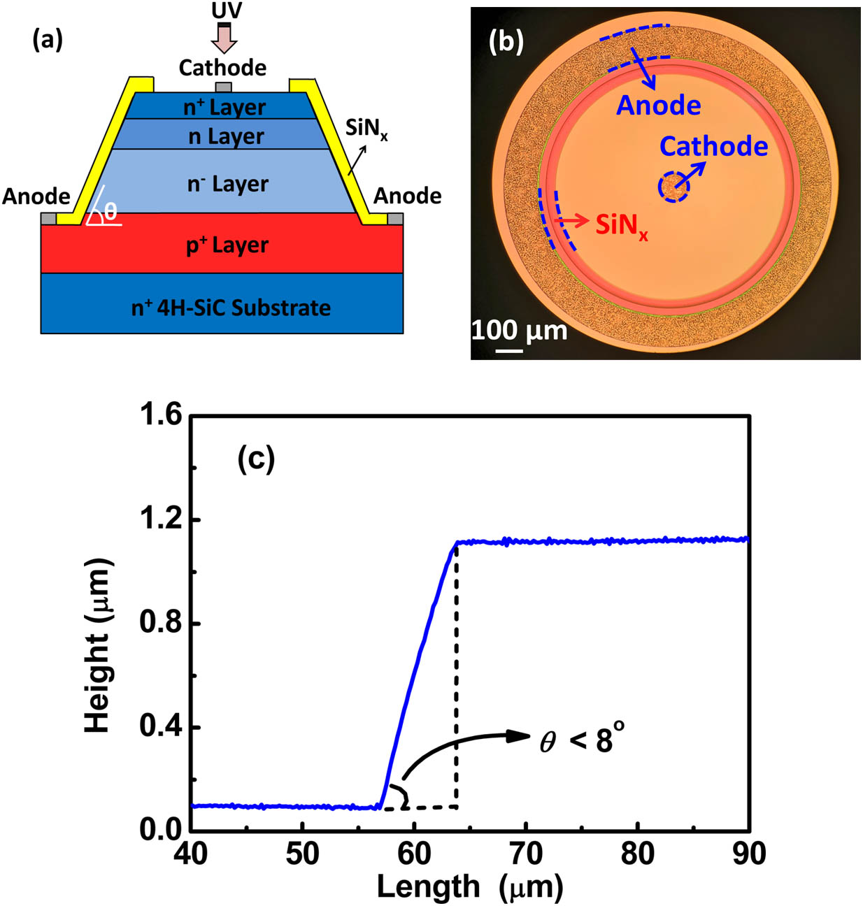
The epitaxial structure of our 4H-SiC p-i-n APDs, which was grown by metal–organic chemical vapor deposition (MOCVD) on an -type 4H-SiC substrate with low defect density, was designed and optimized. In order to obtain ohmic contact, the contact layer is usually highly doped. However, the UV photons will be absorbed by the top highly doped contact layer, reducing the QE of the devices. Therefore, the thickness and doping concentration of the contact layer must be carefully designed. As shown in Fig. 1(a), the epi-structure in this work is composed of a 3 μm layer, a 0.5 μm layer, a 0.2 μm layer, and a 0.1 μm contact layer. The doping concentrations of the corresponding epi-layers from bottom to top are , , , and , respectively. The device fabrication began with the mesa formation etched by inductively coupled plasma (ICP). A positively beveled sidewall () was created for the mesa to suppress the premature edge breakdown. By adopting our proposed variable-temperature photoresist reflow method during the mesa formation process, very smooth mesa sidewalls were obtained, and the process details can be referred to in Ref. [18]. After that, the metal contact stack with Ni (35 nm) /Ti (50 nm) /Al (150 nm) /Au (100 nm) was deposited by e-beam evaporation, which was then annealed at 900°C in ambient for 3 min. Finally, the wafer was passivated by a PECVD layer (500 nm), and the contact and an optical window were opened by removing the layer in the contact and active regions. In order to avoid surface damage in the photosensitive area, the upper and lower parts of the passivation layer were removed carefully by ICP dry etching and chemical wet etching, respectively. Fig. 1(b) gives the top-view photo image of one fabricated 4H-SiC APD with 800 μm diameter, and the profile of the beveled mesa is shown in Fig. 1(c).
Sign up for Chinese Optics Letters TOC. Get the latest issue of Chinese Optics Letters delivered right to you!Sign up now

Figure 1.(a) Schematic structure of the large-area 4H-SiC p-i-n UV APD, where the drawing is not to scale; (b) the top-view image of one fabricated 4H-SiC APD with 800 μm diameter; (c) profile of the beveled mesa with an angle of 8°.
The reverse leakage characteristics of fabricated large-area 4H-SiC APDs were firstly analyzed, and the dark currents of APDs with various diameters are plotted in Fig. 2. As seen from Fig. 2(a), the dark currents of devices with different sizes are very low and limited by the noise floor of the experimental setup, which should be below 10 pA ( for the device with 800 μm diameter) at low reverse bias. Additionally, the avalanche breakdown voltage is very uniform, and premature edge breakdown does not occur, which benefits from the smooth mesa sidewall and high-quality passivation in the sidewall region. However, the dark current near the breakdown voltage starts to increase with the increasing device dimension. In order to investigate the rising dark current at high voltage, dark currents at two different bias voltages (160 V/170 V) are extracted as a function of device size, as illustrated in Fig. 2(b). It is shown that the dark current quadratically depends on the device diameter (), which indicates that the dark current at high reverse voltage is mainly due to bulk leakage rather than surface leakage. There are some possible reasons responsible for the bulk leakage, such as material defects or tunneling. It is considered that the dark current of the p-n or p-i-n structure 4H-SiC APDs near the breakdown voltage is dominated by the trap-assisted tunneling[9]. In our future work, the physical mechanisms of reverse leakage current of our 4H-SiC p-i-n APD devices will be further studied in detail based on the temperature-dependent measurements.
Figure 2.(a) Dark current of fabricated APDs with various sizes; (b) dark current as a function of device diameter at the reverse voltages of 160 V and 170 V.
The device performance of the 800 μm diameter 4H-SiC p-i-n APD for UV detection was investigated at room temperature (see Fig. 3). The characteristics, including dark current () and photocurrent (), are plotted in Fig. 3(a), which is also along with the multiplication gain (). The photocurrent in this work was measured under UV illumination at . As is seen from Fig. 3(a), at low reverse bias voltages for our large-area 4H-SiC p-i-n APD, the dark current is very low (), which is below the measurement limit of the apparatus. The hard avalanche breakdown happens at the reverse voltage around 170 V without premature edge breakdown occurring. A high multiplication gain of is achieved at . The gain is calculated according to , where the unity-gain reference was defined at the reverse voltage of 10 V.
Figure 3.UV detection performance of 800 μm diameter 4H-SiC p-i-n APD: (a) I–V measurement results; (b) spectral response characteristics.
Moreover, the spectral responses of the 4H-SiC p-i-n APD with 800 μm diameter were obtained at 10 V in the UV range from 200 to 400 nm, as depicted in Fig. 3(b). A xenon lamp was adopted as the UV light source for the measurement system, and a silicon-based UV photodetector was used for calibration. The measurement results show that the responsivity of 4H-SiC p-i-n APDs in this work peaks at 0.189 A/W at , and the corresponding unity-gain external QE is 85.5%, which have reached a record high for the reported SiC APDs. The high QE can be attributed to the high quality of epitaxial material as well as the optimized device structure. As mentioned before, besides the absorption layer, the highly doped contact layer can also impact the absorption of photons, especially for the short-wavelength photons. Compared with the QE of 80.5% for the 4H-SiC APD, which has a 0.3 μm -type contact layer (), the maximum QE of the 4H-SiC APD in this work (the contact layer is designed as two layers including a 0.2 μm -type layer with and a 0.1 μm -type layer with ) is increased to 85.5% (not shown here). Therefore, the thickness and doping concentration of each epi-layer must be optimized before 4H-SiC APD fabrication. Additionally, an excellent rejection ratio of UV to visible light () is calculated, which is defined as the ratio of responsivity measured at and .
For performance comparison, the results of various 4H-SiC APDs from other research groups are shown as a function of device diameter together with our samples in Fig. 4. We can see that the fabricated 4H-SiC p-i-n APD in this work has a larger active area, which is advantageous in low-level UV detection applications. Meanwhile, the performance of our device is comparable to or even better than the reported results from other research work at the terms of gain and QE, which can be attributed to the high quality of the passivation layer and epitaxial material, as well as the improved smooth mesa sidewalls.
Figure 4.Comparison of our large-area 4H-SiC p-i-n APD with the results of others’ work.
Finally, UV imaging is demonstrated based on our 4H-SiC p-i-n APD at the reverse bias voltage of 10 V, as shown in Fig. 5. The experimental setup for the UV imaging is shown in Fig. 5(a). The UV light () covered with a mask of the Hebei Semiconductor Research Institute (HSRI) logo was used as the targeted object. An optical chopper was adopted between the target and 4H-SiC p-i-n APD UV detector. The output photoelectric signal (photocurrent) of the UV detector was amplified by a lock-in amplifier and was recorded as the function of coordinates by the scanning displacement stage. Since the UV imaging in this work was demonstrated without lenses, a relatively large-scale targeted object was chosen here. The acquired UV image of the targeted logo is shown in Fig. 5(b), indicating good photocurrent contrast.
Figure 5.UV imaging measurement of our fabricated 4H-SiC p-i-n APD: (a) schematic diagram of the experimental setup; (b) UV photo image of HSRI logo obtained by our 4H-SiC APD-based UV detector.
In conclusion, high-performance large-area 4H-SiC p-i-n visible-blind APDs have been fabricated and investigated for UV detection. Our 4H-SiC APD with large area exhibits a high multiplication gain of , a low dark current of , a record maximum QE of 85.5% at 274 nm, and an excellent UV/visible rejection ratio of at room temperature. The high performance means a very encouraging improvement for solid-state UV detectors based on 4H-SiC APDs with large detection area. The UV imaging based on our 4H-SiC p-i-n APD is also demonstrated for system-level applications, which will be further investigated in our ongoing work in the future.
References
[1] T. Liu, P. Wang, H. Zhang. Chin. Opt. Lett., 13, 040601(2015).
[2] Z. Alaie, S. M. Nejad, M. H. Yousefi. Mater. Sci. Semicond. Process., 29, 16(2015).
[3] Y. Shi, Z. Li, B. Feng, P. Yan, B. Du, H. Zhou, H. Pan, G. Wu. Chin. Opt. Lett., 14, 030401(2016).
[4] J. Kim, M.-H. Ji, T. Detchprohm, J.-H. Ryou, R. D. Dupuis, A. K. Sood, N. K. Dhar. IEEE Photon. Technol. Lett., 27, 642(2015).
[5] M.-H. Ji, J. Kim, T. Detchprohm, Y. Zhu, S.-C. Shen, R. D. Dupuis. IEEE Photon. Technol. Lett., 30, 181(2018).
[6] L. Östlund, Q. Wang, R. Esteve, S. Almqvist, D. Rihtnesberg, S. Reshanov, A. Z. Z. Zhang, J.-K. Lim, M. Bakowski, A. Schöner, W. Kaplan. Phys. Status Solidi C, 9, 1680(2012).
[7] F. Yan, Y. Luo, J. H. Zhao, G. H. Olsen. Electron. Lett., 35, 929(1999).
[8] H.-D. Liu, X. Guo, D. McIntosh, J. C. Campbell. IEEE Photon. Technol. Lett., 18, 2508(2006).
[9] X. Guo, A. L. Beck, Z. Huang, N. Duan, J. C. Campbell, D. Emerson, J. J. Sumakeris. IEEE Trans. Electron Device, 53, 2259(2006).
[10] H.-D. Liu, D. McIntosh, X. Bai, H. Pan, M. Liu, J. C. Campbell, H. Y. Cha. IEEE Photon. Technol. Lett., 20, 1551(2008).
[11] X. Zhou, J. Li, W. Lu, Y. Wang, X. Song, S. Yin, X. Tan, Y. Lü, H. Guo, G. Gu, Z. Feng. Chin. Opt. Lett., 16, 060401(2018).
[12] Q. Zhou, D. McIntosh, H.-D. Liu, J. C. Campbell. IEEE Photon. Technol. Lett., 23, 299(2011).
[13] S. Yang, D. Zhou, H. Lu, D. Chen, F. Ren, R. Zhang, Y. Zheng. IEEE Photon. Technol. Lett., 28, 1185(2016).
[14] A. Vert, S. Soloviev, J. Fronheiser, P. Sandvik. IEEE Photon. Technol. Lett., 20, 1587(2008).
[15] X. Zhou, J. Li, W. Lu, X. Song, S. Yin, Y. Wang, X. Tan, Y. Lv, Z. Feng. IEEE International Conference on Electron Devices and Solid State Circuits(2018).
[16] D. Zhou, F. Liu, H. Lu, D. Chen, F. Ren, R. Zhang, Y. Zheng. IEEE Photon. Technol. Lett., 26, 1136(2014).
[17] L. Li, D. Zhou, F. Liu, H. Lu, F. Ren, D. Chen, R. Zhang, Y. Zheng. IEEE Photon. Technol. Lett., 28, 2526(2016).
[18] X. Zhou, T. Han, Y. Lv, J. Li, W. Lu, Y. Wang, X. Song, X. Tan, S. Liang, Z. Feng, S. Cai. IEEE Electron. Device Lett., 39, 1724(2018).
[19] X. Xin, F. Yan, T. W. Koeth, C. Joseph, J. Hu, J. Wu, J. H. Zhao. Electron. Lett., 41, 1192(2005).
[20] H.-Y. Cha, S. Soloviev, S. Zelakiewicz, P. Waldrab, P. M. Sandvik. Sens. J., 8, 233237(2008).