• Laser & Optoelectronics Progress
  • Vol. 58, Issue 15, 1516026 (2021)
Yuhan Li1, Huapan Xiao2, Hairong Wang1、*, Xiaoya Liang1, Changpeng Li3, Xin Ye3、**, Xiaodong Jiang3, Xinxiang Miao3, Caizhen Yao3, and Laixi Sun3
Author Affiliations
  • 1State Key Laboratory for Manufacturing Systems Engineering, Xi'an Jiaotong University, Xi'an , Shaanxi 710049, China
  • 2College of Mechanical Engineering, Chongqing University, Chongqing 400044, China
  • 3Research Center of Laser Fusion, China Academy of Engineering Physics, Mianyang , Sichuan 621900, China
  • show less
    DOI: 10.3788/LOP202158.1516026 Cite this Article Set citation alerts
    Yuhan Li, Huapan Xiao, Hairong Wang, Xiaoya Liang, Changpeng Li, Xin Ye, Xiaodong Jiang, Xinxiang Miao, Caizhen Yao, Laixi Sun. Review on Wet Etching Technique of Fused Silica Optical Elements[J]. Laser & Optoelectronics Progress, 2021, 58(15): 1516026 Copy Citation Text show less
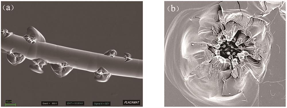
    Damage morphologies on fused silica surface. (a) Damage at scratch edge[20]; (b) morphology of damage initiation site[23]
    Fig. 1. Damage morphologies on fused silica surface. (a) Damage at scratch edge[20]; (b) morphology of damage initiation site[23]
    Laser-induced damage resistance performances before and after fused silica leaching [5]. (a) Damage probability; (b) damage density
    Fig. 2. Laser-induced damage resistance performances before and after fused silica leaching [5]. (a) Damage probability; (b) damage density
    Morphological evolution during etching. (a) Indented pits [41]; (b) ground surface[17]
    Fig. 3. Morphological evolution during etching. (a) Indented pits [41]; (b) ground surface[17]
    Laser damage growth of HF-etched laser damage sites with different sizes after laser irradiation [41].(a)Before irradiation;(b)after irradiation
    Fig. 4. Laser damage growth of HF-etched laser damage sites with different sizes after laser irradiation [41].(a)Before irradiation;(b)after irradiation
    Surface impurity distributions of fused silica measured by TOF-SIMS at different process stages [18]. (a) Before leaching; (b) after HNO3/H2O2 leaching; (c) after HF etching 1 μm; (d) after HF etching 10 μm; (e) after HF etching 50 μm
    Fig. 5. Surface impurity distributions of fused silica measured by TOF-SIMS at different process stages [18]. (a) Before leaching; (b) after HNO3/H2O2 leaching; (c) after HF etching 1 μm; (d) after HF etching 10 μm; (e) after HF etching 50 μm
    Evolution of light intensity distribution on cross-section of optical elements before and after etching [20]. (a) (b) Perpendicular to scratch; (c) (d) parallel to scratch
    Fig. 6. Evolution of light intensity distribution on cross-section of optical elements before and after etching [20]. (a) (b) Perpendicular to scratch; (c) (d) parallel to scratch
    Evolution of damage resistance performance of elements during etching. (a) LIDT[49]; (b) damage probability[42]; (c) damage density[18]
    Fig. 7. Evolution of damage resistance performance of elements during etching. (a) LIDT[49]; (b) damage probability[42]; (c) damage density[18]
    Damage density comparison after AMP2 and AMP3 processing [50]
    Fig. 8. Damage density comparison after AMP2 and AMP3 processing [50]
    SampleComposition (mass fraction)Agitation frequency /kHzLIDT before etching /(J·cm-2LIDT after etching /(J·cm-2LIDT improvement /%Ref.
    Polished surfaceHF (2%)+NH4F (5%)40‒27018.1528.9659.634
    Polished surfaceHF (2.4%)+NH4F (12%)-~17~22~30.037
    Polished surfaceHF (2.4%) +NH4F (12%)1300~20~36~8037
    Polished surfaceHF (1.7%)40‒27022.125.716.338
    Polished surfaceHF (0.4%)+NH4F (12%)40‒27021.326.624.938
    Polished surfaceHF (12%)-16.230.6~8948
    Table 1. LIDT improvement of fused silica under different etching conditions
    SampleComposite techniqueLIDT before etching /(J·cm-2LIDT after etching /(J·cm-2LIDT improvement /%Ref.

    Polished

    surface

    RIE(etching depth of 1 μm)+DCE(etching depth of 3 μm)256616459

    Polished

    surface

    RIE(etching depth of 1 μm)+DCE(etching depth of 3 μm)20.950.814360

    Polished

    surface

    RIE(etching depth of 5 μm)+DCE(etching depth of 3 μm)22.761.116961

    Polished

    surface

    RIE(etching depth of 1.5 μm)+DCE(etching depth of 3 μm)23.252.512662
    ScratchMRF+HF(etching time of 60 min)7.817.812863
    Table 2. LIDT improvement of fused silica processed by composite technique
    Yuhan Li, Huapan Xiao, Hairong Wang, Xiaoya Liang, Changpeng Li, Xin Ye, Xiaodong Jiang, Xinxiang Miao, Caizhen Yao, Laixi Sun. Review on Wet Etching Technique of Fused Silica Optical Elements[J]. Laser & Optoelectronics Progress, 2021, 58(15): 1516026
    Download Citation