• Acta Photonica Sinica
  • Vol. 49, Issue 6, 0604002 (2020)
Yan-xu ZHU*, Yan-xu ZHU*, Zhuang YANG, Hui-hui SONG, Lai-long LI, Zhong YANG, Qi-xuan LI, and Tie-fan HU
Author Affiliations
  • Key Laboratory of Photoelectron Technology Ministry of Education, Beijing University of Technology, Beijing 100124, China
  • show less
    DOI: 10.3788/gzxb20204906.0604002 Cite this Article
    Yan-xu ZHU, Yan-xu ZHU, Zhuang YANG, Hui-hui SONG, Lai-long LI, Zhong YANG, Qi-xuan LI, Tie-fan HU. Preparation and Optimization of Photosensitive Gate GaN-based High Electron Mobility Transistor Devices[J]. Acta Photonica Sinica, 2020, 49(6): 0604002 Copy Citation Text show less
    Schematic diagram of PZT preparation structure
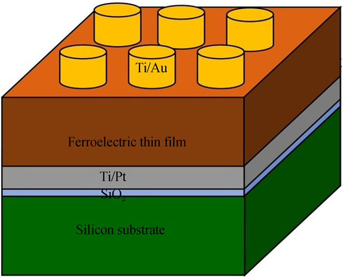
    Fig. 1. Schematic diagram of PZT preparation structure
    SEM morphologies
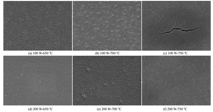
    Fig. 2. SEM morphologies
    XRD analysis chart of different growth conditions
    Fig. 3. XRD analysis chart of different growth conditions
    Analysis of hysteresis loops for different growth conditions
    Fig. 4. Analysis of hysteresis loops for different growth conditions
    Schematic diagram of the PZT/GaN-based HEMT detector structure
    Fig. 5. Schematic diagram of the PZT/GaN-based HEMT detector structure
    Illustration of the steps relevant to the fabrication of the grating electrode GaN-based HEMT device structure
    Fig. 6. Illustration of the steps relevant to the fabrication of the grating electrode GaN-based HEMT device structure
    Dark and UV light output characteristic curves for the tested GaN-based HEMT devices
    Fig. 7. Dark and UV light output characteristic curves for the tested GaN-based HEMT devices
    Optical micrograph of the three kinds of different gate length devices
    Fig. 8. Optical micrograph of the three kinds of different gate length devices
    Characteristic curves of the three different gate length devices
    Fig. 9. Characteristic curves of the three different gate length devices
    Experimental sampleSputtering power/WWorking pressure /PaSputtering time/h
    110011.50
    220010.75
    Table 1. PZT film experimental sample process parameters
    Experimental sampleAnnealing temperature/℃Annealing time/min
    1-A6503
    1-B7003
    1-C7503
    2-A6503
    2-B7003
    2-C7503
    Table 2. Annealing process parameters
    Annealing temperature/℃Saturation polarization/(μC·cm-2)Remnant polarization/(μC·cm-2)Coercive field/(kV·cm-1)
    65030.69.337.0
    70065.320.431.5
    75050.812.433.7
    Table 3. Parameter results of Fig. 4(a)
    Annealing temperature/℃Saturation polarization/(μC·cm-2)Remnant polarization/(μC·cm-2)Coercive field/(kV·cm-1)
    65036.07.132.3
    70084.038.037.3
    75062.617.430.5
    Table 4. Parameter results of Fig. 4(b)
    Sample labelGate length(LG/μm)Gate source spacing(LGS/μm)Gatedrain spacing(LGD/μm)
    A134
    B234
    C334
    Table 5. Device structure parameters for the three different gate lengths
    Yan-xu ZHU, Yan-xu ZHU, Zhuang YANG, Hui-hui SONG, Lai-long LI, Zhong YANG, Qi-xuan LI, Tie-fan HU. Preparation and Optimization of Photosensitive Gate GaN-based High Electron Mobility Transistor Devices[J]. Acta Photonica Sinica, 2020, 49(6): 0604002
    Download Citation