
Yan-xu ZHU, Yan-xu ZHU, Zhuang YANG, Hui-hui SONG, Lai-long LI, Zhong YANG, Qi-xuan LI, Tie-fan HU. Preparation and Optimization of Photosensitive Gate GaN-based High Electron Mobility Transistor Devices[J]. Acta Photonica Sinica, 2020, 49(6): 0604002
- Acta Photonica Sinica
- Vol. 49, Issue 6, 0604002 (2020)
Abstract
Keywords
0 Introduction
Photodetectors are a type of optoelectronic devices which convert optical radiation signals into another form of signals that can be easily received and processed, and are widely used in medical, military, remote sensing imaging, and many other industries[
GaN-basedHigh Electron Mobility Transistors (HEMTs) are epitaxial semiconductor devices, which typically consist of an AlGaN/GaN heterostructure.The AlGaN/GaN heterojunction itself exhibits a spontaneous and piezoelectric polarization. Such strong polarization creates a large amount of 2-dimensional Electron Gas (2-DEG) at the heterojunction, even if the AlGaN control layer is not doped[
The source to drain voltage in the GaN-based HEMT device forms an electric field which acts on the 2-DEG to form an output current. When the gate voltage changes, the concentration and the mobility of the 2-DEG change accordingly. It can be seen that once the source-drain voltage is determined, the source-drain current is dependent only on the gate voltage. Thus, the GaN-based HEMT is a typical gate control device. Researches on HEMT based devices to make detectors focus on the gate control characteristics.In 2015, researchers[
Ferroelectric materials are novel functional materials, and Piezoelectric Ceramic Transducer (PCT) is one of them. Due to their ferroelectric, piezoelectric, thermoelectric, electro-optic, etc., properties, the ferroelectric materials can be used in a variety of device applications, like sensor devices, optoelectronic devices, and various types of memory devices[
In this paper, a new method to change the gate voltage of a HEMT device under light irradiation is proposed to design a new type of photodetector structure. With the aim of combining a GaN-based HEMT with a ferroelectric PZT thin film exhibiting a photovoltaic effect, a PZT thin film is deposited on the gate of the HEMT device to form a novel PZT/GaN-based HEMT detector structure. When the light is irradiated onto the ferroelectric thin film, the latter generates an electric field due to the photovoltaic effect, thereby causing the gate to generate an additional electromotive force. A change in the gate voltage entails a change in the field strength at the AlGaN/GaN interface, that ultimately leads to a change in the 2-DEG[
The following relevant features can be pointed out: 1) Ferroelectric thin films have obvious photovoltaic effects, and the 2-DEG of the GaN-based HEMT device is extremely sensitive to changes in the gate electricfield. Expectedly, the resulting detectors exhibit a high detection rate. 2) The GaN-based HEMT devices are sensitive to input signals, thus reducing the process difficulty due to the thermal insulation of the ferroelectric thin films. 3) A simple planar device structure is required, with no need of micro-motion components, and low vibration/sound interference. 4) The structure is highly expandable, and a wide-spectrum detection can be achieved by changing the photosensitive film, which is favorable for the development of ultraviolet-visible-infrared detectors.
In this paper, based on the gate controlled characteristics of GaN high electron mobility transistors and on the photovoltaic effect in lead zirconate-titanate ferroelectric thin films, a new type of photosensitive layer/HEMT detector structure is proposed. Firstly, in order to prepare films with optimized photovoltaic performance, the surface morphology and ferroelectric properties of PZT films prepared by different sputtering powers and annealing temperatures are analyzed. Secondly, Photosensitive gate GaN HEMT device is prepared, and the output characteristics of the fabricated photosensitive gate PZT/GaN-based HEMT devices are compared to those of pristine HEMTs under both dark condition and 365 nm ultraviolet light.The results show that the new photosensitive gate GaN HEMT detector responds significantly to ultraviolet light.Finally, several HEMT detectors with photosensitive gates of different lengths are also prepared in order to perform a simple optimization of the proposed detector structure.
1 Preparation and analysis of thin films
1.1 Ferroelectric film preparation
Most of the ferroelectrics have perovskite structure, with the molecular formula of ABO3. The target is lead zirconate titanate (PbZr0.52Ti0.48O3, PZT) produced by China New Materials (Beijing) Technology Co., Ltd. The target has a purity of 99.99%, a diameter of 75 mm, and a thickness of 3 mm. The substrate is Pb/Ti/SiO2/Si. A MSP-300B automatic magnetron sputtering coating machine is used. The sputtering furnace is heated to 100 ℃, and the vacuum is 5×10⁻⁴ Pa. Working gas is high purity Ar. Experiments are preliminarily carried out to prepare PZT film samples with two different sputtering powers, and three different annealing conditions. Specific process parameters are listed in Tables 1 and 2, schematic diagram of PZT preparation structure is shown in Fig 1.
| Experimental sample | Sputtering power/W | Working pressure /Pa | Sputtering time/h |
| 1 | 100 | 1 | 1.50 |
| 2 | 200 | 1 | 0.75 |
Table 1. PZT film experimental sample process parameters
| Experimental sample | Annealing temperature/℃ | Annealing time/min |
| 1-A | 650 | 3 |
| 1-B | 700 | 3 |
| 1-C | 750 | 3 |
| 2-A | 650 | 3 |
| 2-B | 700 | 3 |
| 2-C | 750 | 3 |
Table 2. Annealing process parameters
![]()
Figure 1.Schematic diagram of PZT preparation structure
1.2 Test analysis and discussion
1.2.1 Surface topography
As seen in Fig. 2(a)~(c), there is no obvious crystal structure at a sputtering power of 100 W and an annealing temperature of 650 ℃. As the annealing temperature increases to 700 ℃, the grains grow significantly, but the surface of the film is somewhat convex, the film forms a structure other than perovskite[
![]()
Figure 2.SEM morphologies
As it can be seen from Fig. 2(d)~(f), at sputtering power of 200 W and annealing temperature of 650 ℃ the surface of the film is flat, and no significant grain structure appears. At this time, the film does not form a distinct crystal structure. When the annealing temperature is raised to 700 ℃, the film surface exhibits a distinct grain structure, the grain size is uniform, and the spacing is relatively dense. When the annealing temperature finally rises to 750 ℃, the film shows fine cracks. This is because the growth of adjacent grains is hindered by stress, and the stress can not be released, resulting in the occurrence of cracks.
In summary, when the sputtering power is the same, the film annealed at 700 ℃ grows well.And at the same annealing temperature, the surface morphology of the film prepared by 200 W is better. Thus, according to the presented morphological analysis, the optimum growth conditions for the PZT film are a sputtering power of 200 W and an annealing temperature of 700 ℃.
1.2.2 XRD phase analysis
The crystalline properties of the PZT test samples fabricated under different conditions are evaluated by means of X-ray Diffraction (XRD) measurements. It is well-known that a preferred (111)growth orientation is advantageous for the performance of the ferroelectric film[
![]()
Figure 3.XRD analysis chart of different growth conditions
From the reported XRD analysis we can conclude that when the sputtering power is 200 W and the annealing temperature is 700 ℃, the lattice orientation of the film shows the best ferroelectric characteristics. Moreover, from the preparation process analysis, under larger sputtering power the crystal grains generated by the sputtering machine bombarding the target have a higher speed. This, in turn, results in a better adhesion of the crystal grains to the substrate, and the resulting PZT film is more dense.
1.2.3 Hysteresis loop analysis
The three key parameters from the hysteresis loops recorded by the ferroelectric test system are: the coercive field (Ec), the remnant polarization (Pr), and the saturation polarization (Ps)[
![]()
Figure 4.Analysis of hysteresis loops for different growth conditions
| Annealing temperature/℃ | Saturation polarization/(μC·cm-2) | Remnant polarization/(μC·cm-2) | Coercive field/(kV·cm-1) |
| 650 | 30.6 | 9.3 | 37.0 |
| 700 | 65.3 | 20.4 | 31.5 |
| 750 | 50.8 | 12.4 | 33.7 |
Table 3. Parameter results of
| Annealing temperature/℃ | Saturation polarization/(μC·cm-2) | Remnant polarization/(μC·cm-2) | Coercive field/(kV·cm-1) |
| 650 | 36.0 | 7.1 | 32.3 |
| 700 | 84.0 | 38.0 | 37.3 |
| 750 | 62.6 | 17.4 | 30.5 |
Table 4. Parameter results of
We can see From Fig. 4(a) and Table 3, the remnant polarization first increases, and then decreases as the annealing temperature increases. We can draw the same conclusion also from Fig. 4(b) and Table 4. Indeed, as the temperature increases, the perovskite structure begins to grow, so the remnant polarization becomes larger. If the temperature continues to rise, and the Pb element is largely volatilized, resulting in an increase in film defects, and the remnant polarization is thus reduced. Therefore, a balance point can be defined as the best annealing temperature, which results to be 700 ℃.
By comparing the remanent polarization and the coercive electric field of the PZT ferroelectric thin films annealed at 700 ℃ under the two evaluated sputtering power conditions, we can find that the residual polarization and the coercive electric field of the 200 W PZT thin film are greater and smaller, respectively, than those of the 100 W sample. In summary, on the whole, the 200 W sputtering power and 700 ℃ annealing temperature are the best growth conditions for the PZT ferroelectric thin films.
2 Sense grating HEMT device preparation and testing
2.1 Sense grating GaN HEMT preparation process
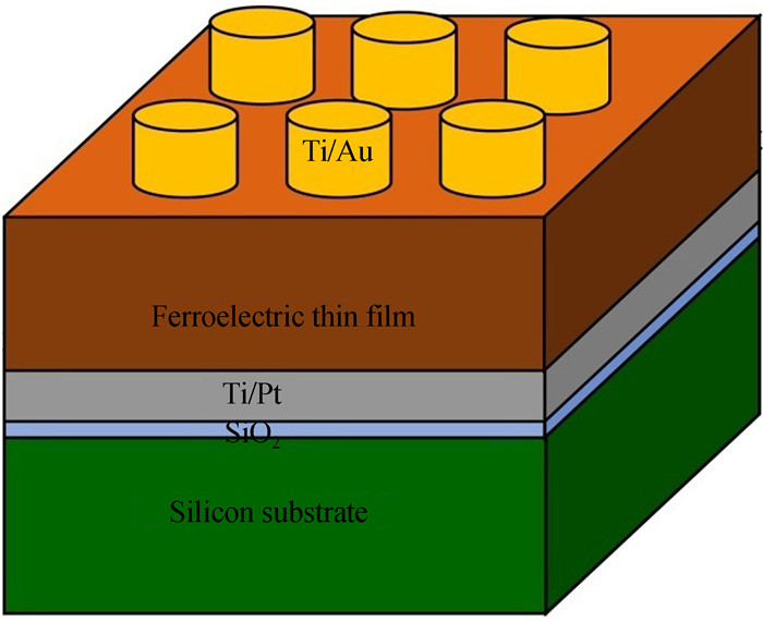
After the analysis of the basic HEMT device and of the optimization procedure for the fabricated PZT thin films, the new PZT/GaN-based HEMT detector structure is discussed in the following. A schematic diagram of the novel device design is shown in Fig. 5.
![]()
Figure 5.Schematic diagram of the PZT/GaN-based HEMT detector structure
The specific steps for the fabrication of the detector structure are schematically illustrated in Fig. 6. They mainly include:cleaning epitaxial, inductively coupled plasma reactive ion etching (Inductively Coupled Plasma) for active area mesa definition, chemical vapor deposition of a SiO2 (200 nm) isolation layer protecting the active region, source and drain electrode sputtering and annealing to form ohmic contacts, Ti/Pt gate electrode sputtering, and PZT grating film growth, sputtering of the upper electrode on the film.
![]()
Figure 6.Illustration of the steps relevant to the fabrication of the grating electrode GaN-based HEMT device structure
2.2 Test analysis
The output characteristics of the HEMT detectors fabricated without and with the photosensitive gate are recorded under both dark condition and 365 nm wavelength UV illumination. In both cases test conditions are: VDS ranging between 0 and 15 V, three sets of VGS voltages are evaluated, namely -3 V, -2.5 V, and -2 V.A 5 W,365 nm Light Emitting Diode (LED) is used as the UV light source, illuminating the device gate during tests.
The output characteristics plotted in Fig. 7 indicate that the tested HEMTs are normally-on (depletion mode) devices. At a given gate voltage VGS, as the source-drain voltage VDS increases, the electron mobility in the channel starts to increase, the source-drain current IDS increases as well, and the device enters the linear region. If the VDS increases further, the electron mobility reaches the maximum, the IDS reaches its maximum value, which is kept almost constant for higher drain-to-source voltages, and the device enters the saturation region. At a given source-drain voltage VDS, as the gate voltage VGS increases, the concentration of 2-DEG starts to increase, the source-drain current IDS increases as well, so among the three evaluated gate voltages, the higher the gate voltage, the higher the device saturation current.During the test, we mainly focus on the changes of saturated source-drain current and saturated source-drain voltage before and after illumination.
![]()
Figure 7.Dark and UV light output characteristic curves for the tested GaN-based HEMT devices
Fig. 7(a) shows the source-drain output characteristics of a pristine HEMT detector, i.e., non-photosensitive grating electrode. Firstly, it can be observed that under UV irradiation, the device source-drain saturation current increases by 1.04 mA and 0.61 mA when VGS is -2 V and -2.5 V, respectively. When VGS is -3 V, the source-drain saturation current remains almost the same. Secondly, the UV light can saturate the source-drain current in advance. Indeed, when VGS is -2 V, the saturation source-drain voltage VDS decreasing by 1.85 V, at most. Thus, the non-photosensitive grating HEMT device does not respond significantly to ultraviolet light.
Fig. 7(b) displays the output characteristics of the photosensitive gate HEMT device. It can be clearly seen that the novel detector structure exhibits a significant response to the UV light. Firstly, the source-drain saturation current increases significantly by about 5.84 mA, 4.38 mA, and 2.34 mA when VGS is -2 V, -2.5 V, and -3 V, respectively. Secondly, the saturation source-drain voltage VDS drop by 3.55 V, at most.
According to the experimental results, it can be concluded that the non-photosensitive grating HEMT device exhibits some response to the UV light, which causes a drop in the device saturation source-drainvoltage, and increases the saturation source-drain current. This is because UV photons can excite electron-hole pairs in the AlGaN/GaN material, thereby increasing the 2-DEG density. However, the response to the UV irradiation of the photosensitive gate HEMT device is markedly larger. Indeed, a PZT ferroelectric thin film is specifically deposited on the metal gate of the GaN-based HEMT device as a light sensing layer. When the light impinges on the gate, the photosensitive PZT layer generates an additional electric field due to the photovoltaic effect, and finally acts on the 2-DEG thereby causing a change in the output current. On the whole, the proposed novel device structure clearly manages to better detect light[
3 Grid optimization
The source-drain output current is obviously affected by the gate voltage. The size of the gate length can regulate the gate voltage to change the output current. Reducing the gate length increases the device transconductance, which in turn increases the gate control capability of the device. However, a too short gate length affects the two-dimensional distribution of the potential under the gate, resulting in a short channel effect[
In this experiment, three different gate length devices are designed. Both the transfer and the output characteristics of the fabricated devices are measured at the same test conditions, under 365 nm wavelength UV light irradiation. The influence of the different gate lengths on the device response is analyzed too. This achieves the goal of optimizing device performance as well as improving device detection efficiency. The device structure parameters relevant to the different gate lengths are summarized in the Table 5. Fig. 8 shows the physical maps of the three devices.
| Sample label | Gate length( | Gate source spacing( | Gatedrain spacing( |
| A | 1 | 3 | 4 |
| B | 2 | 3 | 4 |
| C | 3 | 3 | 4 |
Table 5. Device structure parameters for the three different gate lengths
![]()
Figure 8.Optical micrograph of the three kinds of different gate length devices
In the transfer characteristic curves, VGS varies between -4 V and +2 V. The results are plotted in Fig. 9(a). Clearly, as the gate length increases, the threshold voltage of the HEMT device becomes larger. In the output characteristics, VDS ranges between 0 V and 15 V, and VGS is set to -2 V. The results are displayed in Fig. 9(b).The saturation currents of devices A, B, and C are 17 mA, 20 mA, and 23 mA, respectively. That is, the longer the gate, the smaller the device drain saturation current. Indeed, the longer the gate, the larger the width of the depletion layer below the gate, which causes the 2-DEG concentration to drop here, eventually causing the drain current to drop. Moreover, the increase in gate length leads to an increase in channel resistance, as well as to a longer carrier transport path, and to a knee voltage effect, which all lead to a decrease in the drain saturation current.
![]()
Figure 9.Characteristic curves of the three different gate length devices
The reported experimental results show that the photosensitive gate HEMT device specifically designed as a new type of photodetector not only exhibits a higher sensitivity to light, but also allows for improving the overall detection efficiency by changing its structural parameters. In the future, we can further improve the detection efficiency by improving other structural parameters of the device.
4 Conclusion
In this paper, a novel photosensitive gate GaN HEMT detector structure is proposed, based on the favorable photovoltaic effect in PZT ferroelectric thin films and on the characteristics of GaN HEMT devices. The output characteristics of the photosensitive gate HEMT device are measured under both dark conditions and illumination of ultraviolet light. It is found that the fabricated detector exhibits a significant photoresponse to ultraviolet light. Indeed, under illumination, the output current increases by 5.84 mA, and the saturation voltage drops by 3.55 V, at most. This is because when the light impinges on the photosensitive gate, an additional electric field is generated due to the photovoltaic effect in the PZT layer. This electric field acts on the 2-DEG, and the gate voltage control of the channel is achieved, thereby increasing the output current. Finally, three different gate length photosensitive gate HEMT devices are fabricated. It is found that the longer the gate, the smaller the source-drain output current of the device. This is due to the increase in gate length resulting in a decrease in 2-DEG concentration, and an increase in channel resistance. In summary, the proposed novel photosensitive gate GaN-based HEMT detector structure exhibits a high sensitivity to light. As a future work, the manufacturing process of both the ferroelectric thin film and the HEMT device will be further optimized to improve the detection performance.
References
[8] Jin-lun LI, Shao-hui CUI, Jing ZHANG. Research of InP-based room temperature HEMT terahertz detector enhanced by butterfly antenna. Infrared and Laser Engineering, 48, 131-138(2019).


Set citation alerts for the article
Please enter your email address

© Copyright 2018-2021 | Chinese Laser Press. All Rights Reserved 沪ICP备15018463号-20