
Xinyi Li, Ge Li, Hongbo Lu, Wei Zhang. >35% 5-junction space solar cells based on the direct bonding technique[J]. Journal of Semiconductors, 2021, 42(12): 122701
- Journal of Semiconductors
- Vol. 42, Issue 12, 122701 (2021)
Abstract
1. Introduction
The pursuing of higher efficiencies is always one of the most important activities for photovoltaics community. III–V multijunction solar cells (MJSCs) are the highest efficiency photovoltaic devices yet demonstrated, for both space and terrestrial applications, among all promising technologies. Nowadays over 90% space missions use high efficiency MJSCs as the major power-sources. The higher efficiencies are extremely leveraging for spacecrafts, since they reduce all area-related weights of solar panels required for a given power output, which would reduce the launch cost and/or increase the payloads. Solar cells with efficiencies in excess of 36% have been specifical required for ongoing missions in China’s Lunar Exploration Program (CLEP). It motivates the evolution of the MJSC architectures to achieve higher efficiency, by reducing carrier thermalization losses during energy conversion.
Recently high efficiency devices with four- to six-junction designs have been fabricated through two different pathways termed SBT solar cells and inverted metamorphic (IMM) solar cells, respectively. SBT 5J cells built at Spectrolab have reached world-record one-sun efficiency of 35.8% (~36%) under the standard space spectrum (AM0) and one-sun efficiency of 38.8% under the standard terrestrial spectrum (AM1.5)[
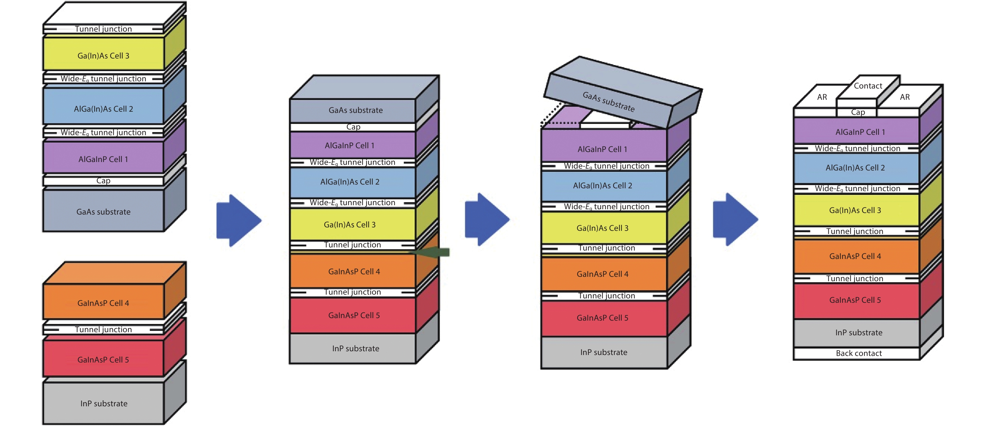
The fabrication of SBT solar cells contains the following processes, as shown in Fig. 1. Subcells are lattice-matched epitaxial grown on suitable substrates (usually GaAs and InP), while top-cells are inverted and grown with etch layers or a sacrificial layer between the substrate and active layers for further convenience. Wafers are then direct semiconductor bonded. After the removal of the one-side growth substrate, the mixture is processed following the standard III–V solar cell device art. The advantage of this approach is that all junctions in the stack are grown lattice-matched and therefore have excellent epitaxial quality, which results in higher efficiencies. Also, the bonding process supports the scale-up to 4-inch or larger wafers, which provides the foundation for further industrial applications.
![]()
Figure 1.(Color online) Fabrication scheme of SBT 5J cells. The arrow indicates the bonding interface.
We have been working on SBT MJSCs from device physics to cell fabrication since 2006. Recently, SBT 5J solar cells with efficiencies in excess of 35% under the space AM0 spectrum are demonstrated. In this paper, some key points for SBT 5J cells are stated, and their appropriate strategies are discussed.
2. Challenges in SBT 5J solar cells
2.1. Suitable subcells for SBT 5J solar cells
2.1.1. Bandgap combination
Based on features of the AM0 spectrum and detailed-balance model, the generally proposed bandgap combination of 5J devices could achieve efficiencies greater than 36% is approximately 2.10/1.70/1.40/1.13/0.88 eV, and it is supposed to produce an open-circuit voltage (Voc) about 4.8 V and a short-circuit current density (Jsc) around 12 mA/cm2. Using experimental bandgap-voltage offsets (Wocs), feasible Vocs around 4.85–4.95 V for such combination could be estimated[
Assuming unity quantum efficiency (QE), the maximum photogenerated current (Jph) in the region from 300 to 900 nm is about 38 mA/cm2 for cells grown on GaAs substrates. For series-stacked T3J, a total Jph of 36 mA/cm2, three-fold of the expected Jsc, is at least required. It implies that the average surface reflectance of T3Js must be controlled below 5%, and also the propagation of light in junctions must be carefully managed to balance the current in each subcell.
Given the fact that internal quantum efficiencies (IQEs) of individual subcells are always less than unity, it demands antireflection coatings (ARCs) with even lower reflectivity to collect as many photons as possible. Therefore, compared with Voc, a Jsc of 12 mA/cm2 is more challenging. The average reflectance of recent state-of-art 36% solar cells in 300–900 nm range has been minimized below 2% to deliver a Jsc of 12 mA/cm2[
An alternative is to narrow the bandgap distance between subcells, by slightly reducing Jsc but increasing Voc to meet efficiencies. Therefore, the bandgap combination, together with ARCs, should be coupled optimized to address requirements from both energy and optical management. As a nature of series-connected stacks, the fill factor (ff) of MJSC is pinned to a little higher value than the poorest ff of subcells. For III–V based subcells, the fill factor usually drops as the bandgap of the absorber layer decreases. Therefore, a scenario of a high-Eg top subcell current-limiting with an extra margin for Jph in low-Eg bottom subcells, would be preferred for bandgap combinations to achieve higher efficiencies.
In addition, the luminescent coupling (LC) behavior complicates the tuning of bandgap combination[
![]()
Figure 2.(Color online) Predicted efficiencies of T3Js containing a GaAs subcell (a) without and (b) with LC. LC coefficient is set to 0.93 during calculation.
Also, parts of radiative photons could be wasted by tunnel diodes with parasitic optical absorption between subcells. Therefore, from the viewpoint of energy conversion, LC is unfavorable for high efficiency, but unavoidable. The cascade LC in multi-bandgap systems, or in MJSCs, makes it difficult to evaluate loss of output voltage and gain of Jph in each subcell, since LC coefficients between subcells are extracted from the correlation of spatial coupled optical distribution and present non-linearities. It maximizes the inaccuracy of predicted efficiency from a given bandgap combination.
The preliminary results suggest that in T3Js containing GaAs subcells, the Eg of the top-cell should be at least larger than 2.1 eV, while the Eg of the mid-cell should be about 1.72 eV. A typical band diagram of such T3J is shown in Fig. 3.
![]()
Figure 3.(Color online) Calculated band diagram for 2.10/1.72/1.42 eV T3J.
2.1.2. High Al% AlGaInP top subcell
In spite of uncertainty of the bandgap combination, top-cells with Eg of 2.1–2.2 eV are well-recognized as better energy harvesting of short-wavelength photons. AlGaInP, with aluminum composition around 20%, is the only option for high-Eg top subcells with material compatibility.
Although AlGaInP has been widely used in microelectronics such as semiconductor lasers, LEDs and microwave power devices[
As the Eg increases, the bandgap offset near the heterojunction surface shrinks, lowering the barrier height for photogenerated carriers. It leads to an increased interface recombination velocity, which is dominated by thermal emission process, and weakens the short-wavelength photon conversion efficiency.
In a traditional p–n junction, the emitter layer of the solar cell plays two distinct roles, not always complementary. On one hand, the emitter layer creates an electric field that separates the electron–hole pairs, and the minority carrier diffusion length in the layer must exceed the emitter thickness to collect as many absorbed carriers as possible. Strong deep-donor levels (DX centers) related to dopants in n-type AlGaInP limit the diffusion length, with the magnitude of the loss increasing with Al%[
By rising the growth temperature, it is generally considered that Al-introduced C- and/or O-related contamination would be reduced and it improves the intrinsic quality of AlGaInP layers. But indium atoms could easily evaporate from the growth surface at high temperature, and also high temperature is not favorable for the incorporation of a volatility p-type Zn dopant. Recently, it is noticed that during the growth of inverted AlGaInP solar cells, higher temperatures lead to abnormal performance deterioration.
On the other hand, the emitter is also required to spread the current laterally to grid fingers so that the current can be collected by external circuit. In this role, a high mobility in concert with a high carrier concentration leading to a low sheet resistance is preferred. For AlGaInP, the mobility is a strong function of Al composition, decreasing by a factor of two over the 0–18% composition range[
To address these problems, a p–n junction containing a doped low-Al% or Al-free emitter and high-Al% weak-p base, or termed reversed heterojunction, is employed to drift generated carriers with a stronger electrical field. But the bandgap offset near the heterojunction interface, together with the diffusion of the dopants can lead to unintended barriers, a valence band well and an emitter barrier, to confine and quench the carriers. It can be partially mitigated by growing a thicker undoped layer, or by grading the aluminum from low-Eg to high-Eg compositions to eliminate the various wells.
2.1.3. Low-Eg quaternary bottom subcells
The general suggested bandgap combinations of bottom two junctions (B2Js) with low-Eg are around 1.13/0.88 eV. Lattice-matched InGaAsP grown on an InP substrate offers tailorable Eg from 0.74 to 1.34 eV, and presents outstanding electrical performances[
Growth temperature plays a critical role during the epitaxy of InGaAsP quaternary. As temperature increases, the pyrolyzation of PH3 is greatly enhanced, and it modifies the incorporation competition between As and P atoms during growth. A slight composition deviation of V-group atoms in the quaternary results in significant variation in both Eg and the lattice-match of epilayers. Experiments reveal that some compressive strain in active layers improves the carrier lifetime in InGaAsP/InP DHs, and benefits the performances of fabricated InGaAsP-based solar cells[
The primary challenge linked to growth temperature is the well-known miscibility gap problem in the InGaAsP quaternary. Besides the potential material quality deterioration caused by defects and dislocations, phase separation during the growth would roughen the surface of epilayers. It leads to failures in the direct bonding process of T3J and B2J wafers.
Fig. 4 plots calculated spinodal isotherms at various temperatures for GaP–GaAs–InP–InAs system based on strictly regular solution approximation[
![]()
Figure 4.Spinodal isotherms for InGaAsP quaternary. The thick solid line indicates compositions lattice-matched to InP.
Metastable regions between spinodal and binodal isotherms provide choices of lower temperature for InGaAsP epitaxy. It lowers growth difficulty for low-Eg quaternary, especially for the bottommost 0.88 eV subcells, but temperature close to binodal isotherms should be avoided for the unstable potential phase.
Meanwhile, since the thickness of subcells in B2J are about 3.5–4.5 μm, the bottom subcell would undergo quite an annealing process when the growth of top subcell is performed. Unintended dopant diffusion during such thermal history would damage abruptness of the interface, resulting in shunt junctions, and consequently poor IV curves for B2J subcells. Therefore, diffusion barriers, or designed doping profiles should be employed to mitigate dopant diffusion during growth.
2.2. Low negative differential resistance (NDR) broadband tunnel diode
To minimize current loss, tunnel diodes connecting subcells should be as transparent as possible to avoid parasitic photon absorption. For T3J, a tunnel diode with Eg above 2.0 eV is at least required to connect 2.1 and 1.7 eV subcells. Considering material compatibility, AlGaInP/AlGaAs with Eg above 2.0 eV are the most promising candidate counterparts for such tunnel diodes.
Although there is little information on its band offsets, a type-II band line-up is predicted for the above-mentioned AlGaInP/AlGaAs heterojunction tunnel diode based on density functional theory (DFT) and transfer principle, as shown in Fig. 5. The tunneling behaviors in tunnel diodes are normally dominated by non-local quantum tunneling between the conduction band and valance band (BTB process). And it couples with defect-related traps-to-bands at the hetero interface (TTB process) in type-II structure. Also, experiments reveal that thermal emission and intra-band tunneling might occur in degenerate AlGaInP/AlGaAs heterojunction. Therefore, it is of great importance to regulate the tunneling probability distribution in the junction, to improve the peak tunneling current and reduce NDR.
![]()
Figure 5.(Color online) Band profile of (a) AlGaInP/AlGaAs tunnel diode, and (b) electrical field and (c, d) tunneling probability distribution in the junction.
For AlGaAs layers, the doping level could easily be above 1 × 1020 cm–3 by decreasing growth temperature and V/III ratio, and increasing the C dopant mole flow. But for AlGaInP layers, the Te dopant must be introduced to obtain a degenerate doping level above 1 × 1019 cm–3 to avoid the band barrier. It brings trades-offs between benefits of neglectable voltage drop across the tunnel diode and risks of memory effect of Te in the following growth.
2.3. Bonding interface
Generally, GaAs and InP bonding layers are implanted on the surface T3J and B2J structures, respectively, to produce a transparent connection to avoid parasitic optical absorption. Due to the minor gap in Eg between GaAs and InP, the band offset near the interface is quite small. By heavy doping, GaAs and InP bonding layers could form counterparts of a tunnel diode, resulting in a low-resistivity interface to avoid barriers for carrier transport, as shown in Fig. 6. It also increases the density of dangling bonds in layers, which enhances van der Waals force in the initial stage of bonding and benefits the reliability of the process.
![]()
Figure 6.(Color online) Schematic device structure after the bonding process.
Previous reports on semiconductor lasers suggest that interface perturbations induced by the bonding process have a minor influence on the light scattering at the interface[
![]()
Figure 7.(Color online) Measured surface reflection and its fitting results.
For the purpose of better optical management in pursuing higher efficiencies, the dispersion behavior of such a mixture, probably an amorphous layer, should be established. It requires tedious sample preparing, measuring and modelling.
3. Our recent progress in SBT 5J cells
Lattice-matched T3J with bandgap combination of 2.1/1.7/1.4 eV is inverted grown on a GaAs substrate. With band and surface engineering, potential barriers induced by surface defects and/or surface passivation are greatly reduced. A Voc of 3.7 V and an ff of 0.86 are obtained under AM0 for 12-cm2 T3J subcell, as shown in Fig. 8(a).
![]()
Figure 8.(Color online)
Lattice-matched B2J with bandgap combination of 1.13/0.88 eV is upright grown on the InP substrate. By introducing zinc diffusion barriers, the fabricated 4-cm2 B2J subcell shows a Voc above 1.2 V and an ff above 0.81 under AM0, as shown in Fig. 8(b).
SBT 5J cells are then fabricated through the direct bonding of T3J and B2J wafers. A broadband ZnS/MgF2 ARC is deposited to minimize reflection loss. Cells are 2 × 2 cm2 in size. Prior to I–V measurements, the spectrum simulator (X-25A, Spectrolab Inc.) is calibrated by multiple reference cells with Eg varied from 2.1 to 0.72 eV to avoid significant spectrum mismatch. All references are standardized using 35km-altitude balloon. Figs. 8(c) and 8(d) display the I–V curve and corrected QE for the best representative cell. It shows an efficiency of 35.39% under AM0 spectrum with a Voc of 4.92 V, a Jsc of 11.37 mA/cm2 and an ff of 0.855, while the world-record SBT 5J cell (4 cm2) from Spectrolab presents a Voc of 4.832 V, a Jsc of 11.77 mA/cm2 and an ff of 0.845[
4. Conclusion
The major key points for fabrication of SBT 5J cells and their appropriate strategies are presented. Integrated effort on structure tunning, band engineering and material tailoring produces the devices with solar energy conversion efficiency above 35%. Compared to Voc, the expected Jsc is much more challenging. With further improvements in optical management, a current boost of 0.5–0.7 mA/cm2 would be achieved in SBT 5J cells, and efficiencies around 36%–37% could be expected.
Acknowledgements
This work is supported by the National Nature Science Foundation of China (Grant No. 62004126), and Shanghai Rising-Star Program (Grant No. 19QB1403800).
References
[1] P T Chiu, D C Law, S B Singer et al. High performance 5J and 6J direct bonded (SBT) space solar cells. 2015 IEEE 42nd Photovoltaic Specialist Conference (PVSC), 1(2015).
[2] P T Chiu, D C Law, R L Woo et al. 35.8% space and 38.8% terrestrial 5J direct bonded cells. 2014 IEEE 40th Photovoltaic Specialist Conference (PVSC), 0011(2014).
[3] P T Chiu, D C Law, R L Woo et al. Direct semiconductor bonded 5J cell for space and terrestrial applications. IEEE J Photovolt, 4, 493(2014).
[4] J F Geisz, R M France, K L Schulte et al. Six-junction III–V solar cells with 47.1% conversion efficiency under 143 Suns concentration. Nat Energy, 5, 326(2020).
[5] J F Geisz, M A Steiner, N Jain et al. Building a six-junction inverted metamorphic concentrator solar cell. IEEE J Photovolt, 8, 626(2018).
[6] R R King, D Bhusari, A Boca et al. Band gap-voltage offset and energy production in next-generation multijunction solar cells. Prog Photovolt: Res Appl, 19, 797(2011).
[7] T Tayagaki, S K Reichmuth, H Helmers et al. Transient analysis of luminescent coupling effects in multi-junction solar cells. J Appl Phys, 124, 183103(2018).
[8] T Tayagaki, R Oshima, Y Shoji et al. Luminescence effects on subcell current-voltage analysis in InGaP/GaAs tandem solar cells. J Photonics Energy, 10, 025504(2020).
[9] S H Lim, J J Li, E H Steenbergen et al. Luminescence coupling effects on multijunction solar cell external quantum efficiency measurement. Prog Photovolt: Res Appl, 21, 344(2013).
[10] H Hamada, M Shono, S Honda et al. AlGaInP visible laser diodes grown on misoriented substrates. IEEE J Quantum Electron, 27, 1483(1991).
[11] M C Wu, J F Lin, M J Jou et al. High reliability of AlGaInP LED's with efficient transparent contacts for spatially uniform light emission. IEEE Electron Device Lett, 16, 482(1995).
[12] M Zaknoune, O Schuler, F Mollot et al. 0.1 μm (Al0.5Ga0.5)0.5In0.5P/In0.2Ga0.8As/GaAs PHEMT grown by gas source molecular beam epitaxy. Electron Lett, 35, 1776(1999).
[13] S Heckelmann, D Lackner, C Karcher et al. Investigations on Al
[14] M A Steiner, R M France, E E Perl et al. Reverse heterojunction (Al)GaInP solar cells for improved efficiency at concentration. IEEE J Photovolt, 10, 487(2020).
[15] H B Lu, X Y Li, W Zhang et al. MOVPE grown 1.0 eV InGaAsP solar cells with bandgap-voltage offset near to ideal radiative recombination limit. Sol Energy Mater Sol Cells, 196, 65(2019).
[16] H B Lu, G Li, X Y Li et al. Small lattice-mismatched InGaAsP: Material characterization and application in solar cells. Chin J Lumin, 41, 351(2020).
[17] K Onabe. Calculation of miscibility gap in quaternary InGaPAs with strictly regular solution approximation. Jpn J Appl Phys, 21, 797(1982).
[18] K Ono, M Takemi. Anomalous behavior of phase separation of InGaAsP on GaAs substrates grown by MOVPE. J Cryst Growth, 298, 41(2007).
[19] R R LaPierre, T Okada, B J Robinson et al. Spinodal-like decomposition of InGaAsP(100) InP grown by gas source molecular beam epitaxy. J Cryst Growth, 155, 1(1995).
[20] R J Ram, J J Dudley, J E Bowers et al. GaAs to InP wafer fusion. J Appl Phys, 78, 4227(1995).


Set citation alerts for the article
Please enter your email address

© Copyright 2018-2021 | Chinese Laser Press. All Rights Reserved 沪ICP备15018463号-20